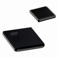
SC28L198A1A,518 NXP Semiconductors, SC28L198A1A,518 Datasheet - Page 47

SC28L198A1A,518
Manufacturer Part Number
SC28L198A1A,518
Description
IC UART OCTAL SOT189-3
Manufacturer
NXP Semiconductors
Type
Octal UART for 3.3 V and 5 V supply voltager
Datasheet
1.SC28L198A1BE557.pdf
(57 pages)
Specifications of SC28L198A1A,518
Number Of Channels
8
Package / Case
84-LCC (J-Lead)
Features
False-start Bit Detection
Fifo's
16 Byte
Voltage - Supply
3.3V, 5V
With Auto Flow Control
Yes
With False Start Bit Detection
Yes
With Modem Control
Yes
With Cmos
Yes
Mounting Type
Surface Mount
Data Rate
0.4608 MBd
Supply Voltage (max)
5.5 V
Supply Voltage (min)
3 V
Supply Current
150 mA
Maximum Operating Temperature
+ 85 C
Minimum Operating Temperature
- 40 C
Mounting Style
SMD/SMT
Operating Supply Voltage
3.3 V or 5 V
Transmit Fifo
16Byte
Receive Fifo
16Byte
Transmitter And Receiver Fifo Counter
No
Operating Supply Voltage (typ)
3.3/5V
Package Type
PLCC
Operating Supply Voltage (max)
5.5V
Operating Supply Voltage (min)
3V
Mounting
Surface Mount
Operating Temperature (min)
-40C
Operating Temperature (max)
85C
Operating Temperature Classification
Industrial
Lead Free Status / RoHS Status
Lead free / RoHS Compliant
Lead Free Status / RoHS Status
Lead free / RoHS Compliant, Lead free / RoHS Compliant
Other names
935261323518
SC28L198A1A-T
SC28L198A1A-T
SC28L198A1A-T
SC28L198A1A-T
1. Timing is illustrated and referenced with respect to W–RN and CEN inputs. Internal read and write activities are controlled by the Sclk as it
2. The minimum time before the rising edge of the next C2 time to stop the next bus cycle. CEN must return high after midpoint of C4 time and
3. Delay is from CEN high in Async mode to IRQN inactive, from end of C4 to IRQN inactive in Sync mode.
4. The minimum frequency values are not tested, but are guaranteed by design.
5. 1MHz specification is for crystal operation.
Philips Semiconductors
AC ELECTRICAL CHARACTERISTICS FOR COMMERCIAL AND INDUSTRIAL (3.3 V)
NOTES:
2006 Aug 10
Fsclk
T/RFsclk
X1 / X2 Communication Crystal Clock
Fx1
X1 L / H
T/RFx1
Counter/Timer Baud Rate Clock (External Clock Input)
FC/T
TC/TLH
TC/TO
DACKN Timing
DAK
DAK
DAK
I/O PORT External Clock
T
G
GPO
SYMBOL
SYMBOL
GPIRTX
Octal UART for 3.3 V and 5 V supply voltage
OUT
generates the several “C” timing as shown in the timing diagrams.
before the C2 time of the next cycle.
5
DLY
DLYA
DLY
4
TDD
Timing
FIGURE
FIGURE
Sclk frequency
Sclk rise/fall time (0.8 to 2.0Volts)
X1 clock frequency
X1 Low / High time
X1 Rise / Fall time
Clock frequency
C/T high and low time
Delay C/T clock external to output pin
DACK low from Sclk C4 rising edge
DACK high from CEN high (ASYNC)
DACK high from C4 end rising edge (SYNC)
GPI to Rx/Tx clock out
RxD setup to I/OP rising edge 1X mode
I/OP falling edge to TxD out 1X mode
GPO valid after write to GPOR
PARAMETER
PARAMETER
47
0.1
1
80
0
20
20
MIN
3.6864
52
15
48
18
18
20
50
2
32
100
LIMITS
TYP
(Continued)
20
5
4
10
8
110
30
30
30
80
70
MAX
SC28L198
Product data sheet
MHz
ns
MHz
ns
ns
MHz
ns
ns
ns
ns
ns
ns
ns
ns
ns
UNIT
UNIT


