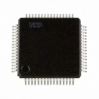
SC16C554DIB64,128 NXP Semiconductors, SC16C554DIB64,128 Datasheet - Page 25

SC16C554DIB64,128
Manufacturer Part Number
SC16C554DIB64,128
Description
IC UART QUAD SOT314-2
Manufacturer
NXP Semiconductors
Datasheet
1.SC16C554DIA68512.pdf
(55 pages)
Specifications of SC16C554DIB64,128
Number Of Channels
4, QUART
Fifo's
16 Byte
Voltage - Supply
2.5V, 3.3V, 5V
With Auto Flow Control
Yes
With Irda Encoder/decoder
Yes
With False Start Bit Detection
Yes
With Modem Control
Yes
With Cmos
Yes
Mounting Type
Surface Mount
Package / Case
64-LQFP
Lead Free Status / RoHS Status
Lead free / RoHS Compliant
Other names
935270063128
SC16C554DIB64-T
SC16C554DIB64-T
SC16C554DIB64-T
SC16C554DIB64-T
Philips Semiconductors
9397 750 13132
Product data
7.3.1 DMA mode
7.3.2 FIFO mode
7.3 FIFO Control Register (FCR)
This register is used to enable the FIFOs, clear the FIFOs, set the transmit/receive
FIFO trigger levels, and select the DMA mode.
Mode 0 (FCR bit 3 = 0):
receive operation, and is similar to the 16C454 mode. Transmit Ready (TXRDY) will
go to a logic 0 whenever an empty transmit space is available in the Transmit Holding
Register (THR). Receive Ready (RXRDY) will go to a logic 0 whenever the Receive
Holding Register (RHR) is loaded with a character.
Mode 1 (FCR bit 3 = 1):
transmit interrupt is set when there are one or more FIFO locations empty. The
receive interrupt is set when the receive FIFO fills to the programmed trigger level.
However, the FIFO continues to fill regardless of the programmed level until the FIFO
is full. RXRDY remains a logic 0 as long as the FIFO fill level is above the
programmed trigger level.
Table 10:
Bit
7:6
5:4
3
Symbol
FCR[7:6]
FCR[5:4]
FCR[3]
FIFO Control Register bits description
Quad UART with 16-byte FIFO and infrared (IrDA) encoder/decoder
Rev. 05 — 10 May 2004
Description
RCVR trigger. These bits are used to set the trigger level for the receive
FIFO interrupt.
An interrupt is generated when the number of characters in the FIFO
equals the programmed trigger level. However, the FIFO will continue to
be loaded until it is full. Refer to
Not used; initialized to logic 0.
DMA mode select.
Transmit operation in mode ‘0’: When the SC16C554/554D is in the
16C450 mode (FIFOs disabled; FCR[0] = logic 0) or in the FIFO mode
(FIFOs enabled; FCR[0] = logic 1; FCR[3] = logic 0), and when there are
no characters in the transmit FIFO or transmit holding register, the
TXRDY pin will be a logic 0. Once active, the TXRDY pin will go to a
logic 1 after the first character is loaded into the transmit holding
register.
Receive operation in mode ‘0’: When the SC16C554/554D is in
mode ‘0’ (FCR[0] = logic 0), or in the FIFO mode (FCR[0] = logic 1;
FCR[3] = logic 0) and there is at least one character in the receive FIFO,
the RXRDY pin will be a logic 0. Once active, the RXRDY pin will go to a
logic 1 when there are no more characters in the receiver.
Logic 0 = Set DMA mode ‘0’ (normal default condition).
Logic 1 = Set DMA mode ‘1’
Set and enable the interrupt for each single transmit or
Set and enable the interrupt in a block mode operation. The
Table
SC16C554/554D
11.
© Koninklijke Philips Electronics N.V. 2004. All rights reserved.
25 of 55


