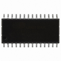
CS8420-CSZ Cirrus Logic Inc, CS8420-CSZ Datasheet - Page 12

CS8420-CSZ
Manufacturer Part Number
CS8420-CSZ
Description
IC SAMPLE RATE CONVERTER 28SOIC
Manufacturer
Cirrus Logic Inc
Type
Sample Rate Converterr
Specifications of CS8420-CSZ
Package / Case
28-SOIC
Applications
CD-R, DAT, DVD, MD, VTR
Mounting Type
Surface Mount
Operating Supply Voltage
5 V
Operating Temperature Range
- 10 C to + 70 C
Mounting Style
SMD/SMT
Resolution
17 bit to 24 bit
Control Interface
3 Wire, Serial
Supply Voltage Range
4.75V To 5.25V
Audio Ic Case Style
SOIC
No. Of Pins
28
Bandwidth
20kHz
Rohs Compliant
Yes
Audio Control Type
Volume
Dc
0841
Lead Free Status / RoHS Status
Lead free / RoHS Compliant
For Use With
598-1782 - EVALUATION BOARD FOR CS8420
Lead Free Status / Rohs Status
Lead free / RoHS Compliant
Other names
598-1125-5
Available stocks
Company
Part Number
Manufacturer
Quantity
Price
Company:
Part Number:
CS8420-CSZ
Manufacturer:
CIRRUS
Quantity:
319
Company:
Part Number:
CS8420-CSZ
Manufacturer:
CIRRUS
Quantity:
9 908
Part Number:
CS8420-CSZ
Manufacturer:
CIRRUS
Quantity:
20 000
Company:
Part Number:
CS8420-CSZ/D1
Manufacturer:
CIRRUS
Quantity:
378
Company:
Part Number:
CS8420-CSZR
Manufacturer:
NICHICON
Quantity:
4 200
4.
The CS8420 can be configured for nine connectiv-
ity alternatives, called data flows. Each data flow
has an associated clocking set-up. Figure 6 shows
the data flow switching, along with the control reg-
ister bits which control the switches; this drawing
only shows the audio data paths for simplicity.
The AESBP switch allows a TTL level, already bi-
phase mark encoded, data stream connected to
RXP to be routed to the TXP and TXN pin drivers.
The TXOFF switch causes the TXP and TXN out-
puts to be driven to ground.
In modes including the SRC function, there are two
audio data related clock domains. One domain in-
cludes the input side of SRC, plus the attached data
source. The second domain includes the output side
of the SRC, plus any attached output ports.
There are two possible clock sources. The first is
known as the recovered clock, is the output of a
PLL, and is connected to the RCMK pin. The input
to the PLL can be either the incoming AES3 data
stream, or the ILRCK word rate clock from the se-
rial audio input port. The second clock is input via
the OMCK pin, and would normally be a crystal
derived stable clock. The Clock Source Control
12
DATA I/O FLOW AND CLOCKING
OPTIONS
ILRCK
ISCLK
SDIN
RXN
RXP
Receiver
Serial
Audio
Input
AES3
Figure 6. Software Mode Audio Data Flow Switching Options
SRCD
Sample
Rate
Converter
Register bits determine which clock is connected to
which domain.
By studying the following drawings, and appropri-
ately setting the Data Flow Control and Clock
Source Control register bits, the CS8420 can be
configured to fit a variety of customer require-
ments.
The following drawings illustrate the possible valid
data flows. The audio data flow is indicated by the
thin lines; the clock routing is indicated by the bold
lines. The register settings for the Data Flow Con-
trol register and the Clock Source Register are also
shown for each data flow. Some of the register set-
tings may appear to be not relevant to the particular
data flow in question, but have been assigned a par-
ticular state. This is done to minimize power con-
sumption. The AESBP data path from the RXP pin
to the AES3 output drivers, and the TXOFF con-
trol, have been omitted for clarity, but are present
and functional in all modes where the AES3 trans-
mitter is in use.
Figures 7 and 8 show audio data entering via the se-
rial audio input port, then passing through the sam-
ple rate converter, and then output both to the serial
audio output port and to the AES3 transmitter. Fig-
ure 7 shows the PLL recovering the input clock
from ILRCK word clock. Figure 8 shows using a
TXD1-0
SPD1-0
AES3
Encoder
AESBP
Serial
Audio
Output
TXOFF
OLRCK
OSCLK
SDOUT
TXP
TXN
CS8420
DS245PP2


