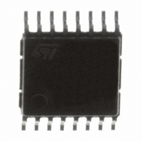
TDA7333013TR STMicroelectronics, TDA7333013TR Datasheet - Page 15

TDA7333013TR
Manufacturer Part Number
TDA7333013TR
Description
IC PROCESSOR RDS/RBDS 16-TSSOP
Manufacturer
STMicroelectronics
Type
RDS/RBDS Signal Processorr
Datasheet
1.TDA7333NTR.pdf
(26 pages)
Specifications of TDA7333013TR
Applications
Radio
Mounting Type
Surface Mount
Package / Case
16-TSSOP
Lead Free Status / RoHS Status
Lead free / RoHS Compliant
Available stocks
Company
Part Number
Manufacturer
Quantity
Price
TDA7333
3.7
This module is used to acquire group and block synchronization of the received RDS data
stream, which is provided in a modified shortened cyclic code. For the theory and
implementation of the modified shortened cyclic code, please refer to the specification of the
radio data system (RDS) EN50067.
It further detects errors in the data stream. Depending on the quality bit information of the
demodulator an error correction is made.
The RDS data bytes are available to the software together with status bits giving an
indication on the reliability of the data.
It also extracts TA information which can be used as interrupt source (see
Programming through serial bus interface
The serial bus interface is used to access the different registers of the chip. It is able to
handle both I
thanks to the pin CSN:
●
●
In both modes, the device is a slave, i.e the clock pin SCL_CLK is only an input for the chip.
Depending on the transfer mode, external pins have alternate functions as following:
Table 7.
Eight registers are available with read or read/write access rights as the following:
Table 8.
The meaning of each bit is described below:
SCL_CLK
SDA_DATAIN
SA_DATAOUT
rds_bd_ctrl[7:0] (see 3.7.6)
rds_corrp[7:0] (see 3.7.3)
rds_bd_h[7:0] (see 3.7.4)
rds_bd_l[7:0] (see 3.7.5)
rds_int[7:0] (see 3.7.1)
rds_qu[7:0] (see 3.7.2)
if the pin CSN is high, the interface operates as an I
if the pin CSN is asserted low, the interface operates as a SPI bus.
sinc4reg[7:0]
testreg[7:0]
Pin
Register
External pins alternate functions
Registers description
2
C and SPI transfer protocols, the selection between the two modes is done
CLK (serial clock)
DATAIN (data input)
DATAOUT (data output)
Function in SPI mode (CSN =0)
read/write
read/write
read/write
read/write
Access
rights
read
read
read
read
Interrupt source setting, sync., bne information
Quality counter, actual block name
Error correction status, buffer ovf information
High byte of current RDS block
Low byte of current RDS block
Frequency, quality sensitivity, demodulator pll settings
Sinc4 filter settings (for internal use only)
Test modes (for internal use only)
2
SCL (serial clock)
SDA (data line)
SA (slave address)
C bus.
Function in I
Function
Functional description
2
C mode (CSN=1)
Chapter
3.7.1).
15/26


