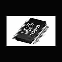
LPC1112FDH28 NXP Semiconductors, LPC1112FDH28 Datasheet - Page 38

LPC1112FDH28
Manufacturer Part Number
LPC1112FDH28
Description
The LPC1112FDH28 is an ARM Cortex-M0 based, low-cost 32-bit MCU, designed for 8/16-bit microcontroller applications, offering performance, low power, simple instruction set and memory addressing together with reduced code size compared to existing 8/
Manufacturer
NXP Semiconductors
Datasheet
1.LPC1110FD20.pdf
(103 pages)
Available stocks
Company
Part Number
Manufacturer
Quantity
Price
Part Number:
LPC1112FDH28
Manufacturer:
TI/德州仪器
Quantity:
20 000
Part Number:
LPC1112FDH28/102:5
Manufacturer:
NXP/恩智浦
Quantity:
20 000
NXP Semiconductors
Table 12.
[1]
[2]
[3]
[4]
[5]
[6]
LPC111X
Product data sheet
Symbol
V
XTALIN
XTALOUT
V
DD
SS
Pin state at reset for default function: I = Input; O = Output; PU = internal pull-up enabled (pins pulled up to full V
IA = inactive, no pull-up/down enabled.
See
reset the chip and wake up from Deep power-down mode. An external pull-up resistor is required on this pin for the Deep power-down
mode.
5 V tolerant pad providing digital I/O functions with configurable pull-up/pull-down resistors and configurable hysteresis (see
I
5 V tolerant pad providing digital I/O functions with configurable pull-up/pull-down resistors, configurable hysteresis, and analog input.
When configured as a ADC input, digital section of the pad is disabled, and the pin is not 5 V tolerant (see
When the system oscillator is not used, connect XTALIN and XTALOUT as follows: XTALIN can be left floating or can be grounded
(grounding is preferred to reduce susceptibility to noise). XTALOUT should be left floating.
2
C-bus pads compliant with the I
Figure 46
LPC1100XL series: LPC1111/12/13/14 pin description table (HVQFN33 package)
for the reset pad configuration. RESET functionality is not available in Deep power-down mode. Use the WAKEUP pin to
Pin
6; 29 -
4
5
33
[6]
[6]
Start
logic
input
-
-
-
2
C-bus specification for I
Type Reset
I
I
O
-
All information provided in this document is subject to legal disclaimers.
state
[1]
-
-
-
-
Rev. 7 — 1 March 2012
Description
3.3 V supply voltage to the internal regulator, the external rail, and the
ADC. Also used as the ADC reference voltage.
Input to the oscillator circuit and internal clock generator circuits. Input
voltage must not exceed 1.8 V.
Output from the oscillator amplifier.
Thermal pad. Connect to ground.
2
C standard mode and I
LPC1110/11/12/13/14/15
2
C Fast-mode Plus.
32-bit ARM Cortex-M0 microcontroller
…continued
Figure
DD
© NXP B.V. 2012. All rights reserved.
45).
level (V
DD
Figure
= 3.3 V));
38 of 103
45).


