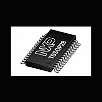
LPC1112FDH28 NXP Semiconductors, LPC1112FDH28 Datasheet - Page 44

LPC1112FDH28
Manufacturer Part Number
LPC1112FDH28
Description
The LPC1112FDH28 is an ARM Cortex-M0 based, low-cost 32-bit MCU, designed for 8/16-bit microcontroller applications, offering performance, low power, simple instruction set and memory addressing together with reduced code size compared to existing 8/
Manufacturer
NXP Semiconductors
Datasheet
1.LPC1110FD20.pdf
(103 pages)
Available stocks
Company
Part Number
Manufacturer
Quantity
Price
Part Number:
LPC1112FDH28
Manufacturer:
TI/德州仪器
Quantity:
20 000
Part Number:
LPC1112FDH28/102:5
Manufacturer:
NXP/恩智浦
Quantity:
20 000
NXP Semiconductors
LPC111X
Product data sheet
7.10.1 Features
7.11.1 Features
7.10 I
7.11 10-bit ADC
The LPC1110/11/12/13/14/15 contain one I
Remark: Part LPC1112FDH20/102 does not contain the I
The I
(SCL) and a Serial DAta line (SDA). Each device is recognized by a unique address and
can operate as either a receiver-only device (e.g., an LCD driver) or a transmitter with the
capability to both receive and send information (such as memory). Transmitters and/or
receivers can operate in either master or slave mode, depending on whether the chip has
to initiate a data transfer or is only addressed. The I
controlled by more than one bus master connected to it.
The LPC1110/11/12/13/14/15 contain one ADC. It is a single 10-bit successive
approximation ADC with eight channels.
2
•
•
•
•
•
•
•
•
•
•
•
•
•
•
•
•
•
•
•
C-bus serial I/O controller
Master or slave operation
8-frame FIFOs for both transmit and receive
4-bit to 16-bit frame
The I
I
Easy to configure as master, slave, or master/slave.
Programmable clocks allow versatile rate control.
Bidirectional data transfer between masters and slaves.
Multi-master bus (no central master).
Arbitration between simultaneously transmitting masters without corruption of serial
data on the bus.
Serial clock synchronization allows devices with different bit rates to communicate via
one serial bus.
Serial clock synchronization can be used as a handshake mechanism to suspend and
resume serial transfer.
The I
The I
10-bit successive approximation ADC.
Input multiplexing among 8 pins.
Power-down mode.
Measurement range 0 V to V
10-bit conversion time 2.44 s (up to 400 kSamples/s).
Burst conversion mode for single or multiple inputs.
2
2
C-bus interface also supports Fast-mode Plus with bit rates up to 1 Mbit/s.
C-bus is bidirectional for inter-IC control using only two wires: a Serial Clock Line
2
2
2
C-interface is a standard I
C-bus can be used for test and diagnostic purposes.
C-bus controller supports multiple address recognition and a bus monitor mode.
All information provided in this document is subject to legal disclaimers.
Rev. 7 — 1 March 2012
DD
.
2
C-bus compliant interface with open-drain pins. The
LPC1110/11/12/13/14/15
2
C-bus controller.
32-bit ARM Cortex-M0 microcontroller
2
C is a multi-master bus and can be
2
C-bus controller.
© NXP B.V. 2012. All rights reserved.
44 of 103


