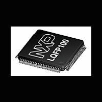
LPC12D27FBD100 NXP Semiconductors, LPC12D27FBD100 Datasheet - Page 9

LPC12D27FBD100
Manufacturer Part Number
LPC12D27FBD100
Description
The LPC12D27FBD100 is a ARM Cortex-M0 based microcontroller for embedded applications featuring a high level of integration and low power consumption
Manufacturer
NXP Semiconductors
Datasheet
1.LPC12D27FBD100.pdf
(46 pages)
Available stocks
Company
Part Number
Manufacturer
Quantity
Price
Company:
Part Number:
LPC12D27FBD100/301
Manufacturer:
NXP Semiconductors
Quantity:
10 000
NXP Semiconductors
Table 3.
LPC12D27
Product data sheet
Symbol
PIO0_6/RI0/
CT32B1_CAP0/
CT32B1_MAT0
PIO0_7/CTS0/
CT32B1_CAP1/
CT32B1_MAT1
PIO0_8/RXD1
/CT32B1_CAP2/
CT32B1_MAT2
PIO0_9/TXD1/
CT32B1_CAP3/
CT32B1_MAT3
PIO0_10/SCL
PIO0_11/SDA/
CT16B0_CAP0/
CT16B0_MAT0
PIO0_12/CLKOUT/
CT16B0_CAP1/
CT16B0_MAT1
RESET/PIO0_13
PIO0_14/SCK
LPC12D27 LQFP100 pin description
Pin
12
13
14
15
17
18
19
20
21
[2]
[2]
[2]
[2]
[3]
[3]
[7]
[4]
[2]
Start
logic
input
yes
yes
yes
yes
yes
yes
no
no
no
Reset
state
[1]
I; IA
I; IA
I; PU
I; PU
I; PU
I; PU
I; PU
I; PU
I; PU
All information provided in this document is subject to legal disclaimers.
Rev. 1 — 20 September 2011
Type
I/O
I
I
O
I/O
I
I
O
I/O
I
I
O
I/O
O
I
O
I/O
I/O
I/O
I/O
I
O
I/O
O
I
O
I
I/O
I/O
I/O
…continued
Description
PIO0_6 — General purpose digital input/output pin. Also serves
as wake-up pin from Deep-sleep mode.
RI0 — Ring Indicator input for UART0.
CT32B1_CAP0 — Capture input, channel 0 for 32-bit timer 1.
CT32B1_MAT0 — Match output, channel 0 for 32-bit timer 1.
PIO0_7 — General purpose digital input/output pin. Also serves
as wake-up pin from Deep-sleep mode.
CTS0 — Clear To Send input for UART0.
CT32B1_CAP1 — Capture input, channel 1 for 32-bit timer 1.
CT32B1_MAT1 — Match output, channel 1 for 32-bit timer 1.
PIO0_8 — General purpose digital input/output pin. Also serves
as wake-up pin from Deep-sleep mode.
RXD1 — Receiver input for UART1.
CT32B1_CAP2 — Capture input, channel 2 for 32-bit timer 1.
CT32B1_MAT2 — Match output, channel 2 for 32-bit timer 1.
PIO0_9 — General purpose digital input/output pin. Also serves
as wake-up pin from Deep-sleep mode.
TXD1 — Transmitter output for UART1.
CT32B1_CAP3 — Capture input, channel 3 for 32-bit timer 1.
CT32B1_MAT3 — Match output, channel 3 for 32-bit timer 1.
PIO0_10 — General purpose digital input/output pin. Also serves
as wake-up pin from Deep-sleep mode.
SCL — I
PIO0_11 — General purpose digital input/output pin. Also serves
as wake-up pin from Deep-sleep mode.
SDA — I
CT16B0_CAP0 — Capture input, channel 0 for 16-bit timer 0.
CT16B0_MAT0 — Match output, channel 0 for 16-bit timer 0.
PIO0_12 — General purpose digital input/output pin. A LOW
level on this pin in during reset starts the ISP command handler.
High-current output driver.
CLKOUT — Clock out pin.
CT16B0_CAP1 — Capture input, channel 0 for 16-bit timer 0.
CT16B0_MAT1 — Match output, channel 1 for 16-bit timer 0.
RESET — External reset input: A LOW on this pin resets the
device, causing I/O ports and peripherals to take on their default
states, and processor execution to begin at address 0.
PIO0_13 — General purpose digital input/output pin.
PIO0_14 — General purpose digital input/output pin.
SCK — Serial clock for SSP.
2
2
C-bus clock input/output.
C-bus data input/output.
32-bit ARM Cortex-M0 microcontroller
LPC12D27
© NXP B.V. 2011. All rights reserved.
9 of 46


