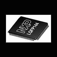
LPC1788FBD144 NXP Semiconductors, LPC1788FBD144 Datasheet - Page 13

LPC1788FBD144
Manufacturer Part Number
LPC1788FBD144
Description
The LPC1788 is a Cortex-M3 microcontroller for embedded applications featuring a high level of integration and low power consumption at frequencies of 120 MHz
Manufacturer
NXP Semiconductors
Datasheet
1.LPC1774FBD144.pdf
(120 pages)
Available stocks
Company
Part Number
Manufacturer
Quantity
Price
Company:
Part Number:
LPC1788FBD144
Manufacturer:
ELPIDA
Quantity:
1 043
Part Number:
LPC1788FBD144
Manufacturer:
NXP/恩智浦
Quantity:
20 000
NXP Semiconductors
Table 3.
Not all functions are available on all parts. See
pins).
LPC178X_7X
Objective data sheet
Symbol
P0[11]
P0[12]
P0[13]
P0[14]
P0[15]
P0[16]
Pin description
100 R14
41
45
69
128 J16
130 J14
R1
R2
T7
…continued
J4
P12
J5
M5
H13 89
H14 90
70
29
32
48
[3]
[5]
[5]
[3]
[3]
[3]
All information provided in this document is subject to legal disclaimers.
I;
PU
I;
PU
I;
PU
I;
PU
I;
PU
I;
PU
Table 2
Rev. 3 — 27 December 2011
I/O
I
I/O
O
-
-
-
-
I/O
O
I/O
I
I/O
O
I/O
I
I/O
O
I/O
O
I/O
O
I/O
I/O
I
I/O
(Ethernet, USB, LCD, QEI, SD/MMC, DAC pins) and
Description
P0[11] — General purpose digital input/output pin.
U2_RXD — Receiver input for UART2.
I2C2_SCL — I
specialized I2C pad).
T3_MAT1 — Match output for Timer 3, channel 1.
R — Function reserved.
R — Function reserved.
R — Function reserved.
R — Function reserved.
P0[12] — General purpose digital input/output pin.
USB_PPWR2 — Port Power enable signal for USB port 2.
SSP1_MISO — Master In Slave Out for SSP1.
ADC0_IN[6] — A/D converter 0, input 6. When configured as an
ADC input, the digital function of the pin must be disabled.
P0[13] — General purpose digital input/output pin.
USB_UP_LED2 — USB port 2 GoodLink LED indicator. It is
LOW when the device is configured (non-control endpoints
enabled), or when the host is enabled and has detected a
device on the bus. It is HIGH when the device is not configured,
or when host is enabled and has not detected a device on the
bus, or during global suspend. It transitions between LOW and
HIGH (flashes) when the host is enabled and detects activity on
the bus.
SSP1_MOSI — Master Out Slave In for SSP1.
ADC0_IN[7] — A/D converter 0, input 7. When configured as an
ADC input, the digital function of the pin must be disabled.
P0[14] — General purpose digital input/output pin.
USB_HSTEN2 — Host Enabled status for USB port 2.
SSP1_SSEL — Slave Select for SSP1.
USB_CONNECT2 — SoftConnect control for USB port 2.
Signal used to switch an external 1.5 k resistor under software
control. Used with the SoftConnect USB feature.
P0[15] — General purpose digital input/output pin.
U1_TXD — Transmitter output for UART1.
SSP0_SCK — Serial clock for SSP0.
P0[16] — General purpose digital input/output pin.
U1_RXD — Receiver input for UART1.
SSP0_SSEL — Slave Select for SSP0.
2
C2 clock input/output (this pin does not use a
32-bit ARM Cortex-M3 microcontroller
LPC178x/7x
© NXP B.V. 2011. All rights reserved.
Table 7
13 of 120
(EMC


