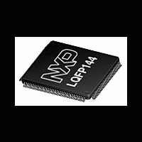
LPC1788FBD144 NXP Semiconductors, LPC1788FBD144 Datasheet - Page 25

LPC1788FBD144
Manufacturer Part Number
LPC1788FBD144
Description
The LPC1788 is a Cortex-M3 microcontroller for embedded applications featuring a high level of integration and low power consumption at frequencies of 120 MHz
Manufacturer
NXP Semiconductors
Datasheet
1.LPC1774FBD144.pdf
(120 pages)
Available stocks
Company
Part Number
Manufacturer
Quantity
Price
Company:
Part Number:
LPC1788FBD144
Manufacturer:
ELPIDA
Quantity:
1 043
Part Number:
LPC1788FBD144
Manufacturer:
NXP/恩智浦
Quantity:
20 000
NXP Semiconductors
Table 3.
Not all functions are available on all parts. See
pins).
LPC178X_7X
Objective data sheet
Symbol
P2[11]
P2[12]
P2[13]
P2[14]
Pin description
108 T17
106 N14
102 T16
91
R12
…continued
N14 73
-
M12 75
M11 71
-
[10]
[10]
[10]
[3]
All information provided in this document is subject to legal disclaimers.
I;
PU
I;
PU
I;
PU
I;
PU
Table 2
Rev. 3 — 27 December 2011
I/O
I
I/O
I/O
-
-
-
O
I/O
I
I/O
I/O
O
O
O
O
I/O
I
I/O
I/O
-
O
O
O
I/O
O
I/O
I
(Ethernet, USB, LCD, QEI, SD/MMC, DAC pins) and
Description
P2[11] — General purpose digital input/output pin. This pin
includes a 5 ns input glitch filter.
EINT1 — External interrupt 1 input.
SD_DAT[1] — Data line 1 for SD card interface.
I2S_TX_SCK — Transmit Clock. It is driven by the master and
received by the slave. Corresponds to the signal SCK in the
I
R — Function reserved.
R — Function reserved.
R — Function reserved.
LCD_CLKIN — LCD clock.
P2[12] — General purpose digital input/output pin. This pin
includes a 5 ns input glitch filter.
EINT2 — External interrupt 2 input.
SD_DAT[2] — Data line 2 for SD card interface.
I2S_TX_WS — Transmit Word Select. It is driven by the master
and received by the slave. Corresponds to the signal WS in the
I
LCD_VD[4] — LCD data.
LCD_VD[3] — LCD data.
LCD_VD[8] — LCD data.
LCD_VD[18] — LCD data.
P2[13] — General purpose digital input/output pin. This pin
includes a 5 ns input glitch filter.
EINT3 — External interrupt 3 input.
SD_DAT[3] — Data line 3 for SD card interface.
I2S_TX_SDA — Transmit data. It is driven by the transmitter
and read by the receiver. Corresponds to the signal SD in the
I
R — Function reserved.
LCD_VD[5] — LCD data.
LCD_VD[9] — LCD data.
LCD_VD[19] — LCD data.
P2[14] — General purpose digital input/output pin.
EMC_CS2 — LOW active Chip Select 2 signal.
I2C1_SDA — I
specialized I2C pad).
T2_CAP0 — Capture input for Timer 2, channel 0.
2
2
2
S-bus specification.
S-bus specification.
S-bus specification.
2
C1 data input/output (this pin does not use a
32-bit ARM Cortex-M3 microcontroller
LPC178x/7x
© NXP B.V. 2011. All rights reserved.
Table 7
25 of 120
(EMC


