LPC1820FET100 NXP Semiconductors, LPC1820FET100 Datasheet - Page 16
LPC1820FET100
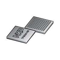
Manufacturer Part Number
LPC1820FET100
Description
The LPC1820FET100 is a high-performance, cost-effective Cortex-M3 microcontroller featuring 168 kB of SRAM, and advanced peripherals including High Speed USB 2
Manufacturer
NXP Semiconductors
Datasheet
1.LPC1810FBD144.pdf
(157 pages)
Available stocks
Company
Part Number
Manufacturer
Quantity
Price
Company:

Part Number:
LPC1820FET100
Manufacturer:
Signetics
Quantity:
45


NXP Semiconductors
Table 3.
LCD, Ethernet, USB0, and USB1 functions are not available on all parts. See
LPC1850_30_20_10
Preliminary data sheet
Symbol
P2_3
P2_4
P2_5
Pin description
J12
K11
K14
x
x
x
…continued
D8
D9
D10 131 91
127 87
128 88
All information provided in this document is subject to legal disclaimers.
Rev. 3.1 — 15 December 2011
57
58
61
[4]
[4]
[4]
I; PU -
I; PU -
I; PU -
I/O I2C1_SDA — I
O
I
I/O GPIO5[3] — General purpose digital input/output pin.
-
O
O
I/O I2C1_SCL — I
I
I
I/O GPIO5[4] — General purpose digital input/output pin.
-
O
O
I
I
I
I/O GPIO5[5] — General purpose digital input/output pin.
-
O
O
Description
R — Function reserved.
not use a specialized I
U3_TXD — Transmitter output for USART3.
CTIN_1 — SCT input 1. Capture input 1 of timer 0.
Capture input 1 of timer 2.
R — Function reserved.
T3_MAT0 — Match output 0 of timer 3.
USB0_PPWR — VBUS drive signal (towards
external charge pump or power management unit);
indicates that VBUS must be driven (active HIGH).
Add a pull-down resistor to disable the power switch
at reset. This signal has opposite polarity compared
to the USB_PPWR used on other NXP LPC parts.
R — Function reserved.
not use a specialized I
U3_RXD — Receiver input for USART3.
CTIN_0 — SCT input 0. Capture input 0 of timer 0, 1,
2, 3.
R — Function reserved.
T3_MAT1 — Match output 1 of timer 3.
USB0_PWR_FAULT — Port power fault signal
indicating overcurrent condition; this signal monitors
over-current on the USB bus (external circuitry
required to detect over-current condition).
R — Function reserved.
CTIN_2 — SCT input 2. Capture input 2 of timer 0.
USB1_VBUS — Monitors the presence of USB1 bus
power.
Note: This signal must be HIGH for USB reset to
occur.
ADCTRIG1 — ADC trigger input 1.
R — Function reserved.
T3_MAT2 — Match output 2 of timer 3.
USB0_IND0 — USB0 port indicator LED control
output 0.
Table
32-bit ARM Cortex-M3 microcontroller
LPC1850/30/20/10
2.
2
2
C1 clock input/output (this pin does
C1 data input/output (this pin does
2
2
C pad).
C pad).
© NXP B.V. 2011. All rights reserved.
16 of 157
Related parts for LPC1820FET100
Image
Part Number
Description
Manufacturer
Datasheet
Request
R

Part Number:
Description:
NXP Semiconductors designed the LPC2420/2460 microcontroller around a 16-bit/32-bitARM7TDMI-S CPU core with real-time debug interfaces that include both JTAG andembedded trace
Manufacturer:
NXP Semiconductors
Datasheet:

Part Number:
Description:
NXP Semiconductors designed the LPC2458 microcontroller around a 16-bit/32-bitARM7TDMI-S CPU core with real-time debug interfaces that include both JTAG andembedded trace
Manufacturer:
NXP Semiconductors
Datasheet:
Part Number:
Description:
NXP Semiconductors designed the LPC2468 microcontroller around a 16-bit/32-bitARM7TDMI-S CPU core with real-time debug interfaces that include both JTAG andembedded trace
Manufacturer:
NXP Semiconductors
Datasheet:
Part Number:
Description:
NXP Semiconductors designed the LPC2470 microcontroller, powered by theARM7TDMI-S core, to be a highly integrated microcontroller for a wide range ofapplications that require advanced communications and high quality graphic displays
Manufacturer:
NXP Semiconductors
Datasheet:
Part Number:
Description:
NXP Semiconductors designed the LPC2478 microcontroller, powered by theARM7TDMI-S core, to be a highly integrated microcontroller for a wide range ofapplications that require advanced communications and high quality graphic displays
Manufacturer:
NXP Semiconductors
Datasheet:
Part Number:
Description:
The Philips Semiconductors XA (eXtended Architecture) family of 16-bit single-chip microcontrollers is powerful enough to easily handle the requirements of high performance embedded applications, yet inexpensive enough to compete in the market for hi
Manufacturer:
NXP Semiconductors
Datasheet:
Part Number:
Description:
The XA-S3 device is a member of Philips Semiconductors? XA(eXtended Architecture) family of high performance 16-bitsingle-chip microcontrollers
Manufacturer:
NXP Semiconductors
Datasheet:

Part Number:
Description:
The NXP BlueStreak LH75401/LH75411 family consists of two low-cost 16/32-bit System-on-Chip (SoC) devices
Manufacturer:
NXP Semiconductors
Datasheet:
Part Number:
Description:
The NXP LPC3130/3131 combine an 180 MHz ARM926EJ-S CPU core, high-speed USB2
Manufacturer:
NXP Semiconductors
Datasheet:
Part Number:
Description:
The NXP LPC3141 combine a 270 MHz ARM926EJ-S CPU core, High-speed USB 2
Manufacturer:
NXP Semiconductors
Part Number:
Description:
The NXP LPC3143 combine a 270 MHz ARM926EJ-S CPU core, High-speed USB 2
Manufacturer:
NXP Semiconductors

Part Number:
Description:
The NXP LPC3152 combines an 180 MHz ARM926EJ-S CPU core, High-speed USB 2
Manufacturer:
NXP Semiconductors
Part Number:
Description:
The NXP LPC3154 combines an 180 MHz ARM926EJ-S CPU core, High-speed USB 2
Manufacturer:
NXP Semiconductors

Part Number:
Description:
Standard level N-channel enhancement mode Field-Effect Transistor (FET) in a plastic package using NXP High-Performance Automotive (HPA) TrenchMOS technology
Manufacturer:
NXP Semiconductors
Datasheet: