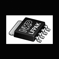
PSMN3R2-25YLC NXP Semiconductors, PSMN3R2-25YLC Datasheet - Page 9

PSMN3R2-25YLC
Manufacturer Part Number
PSMN3R2-25YLC
Description
Logic level enhancement mode N-channel MOSFET in LFPAK package
Manufacturer
NXP Semiconductors
Datasheet
1.PSMN3R2-25YLC.pdf
(15 pages)
NXP Semiconductors
PSMN3R2-25YLC
Product data sheet
Fig 12. Drain-source on-state resistance as a function
Fig 14. Gate charge waveform definitions
R
(mΩ)
DS on
16
12
8
4
0
of drain current; typical values
0
V
V
V
V
GS(pl)
DS
GS(th)
GS
20
Q
2.6
GS1
I
Q
D
GS
40
Q
GS2
2.8
Q
G(tot)
60
Q
GD
N-channel 25 V 3.4 mΩ logic level MOSFET in LFPAK using NextPower
V
3.0
GS
80
All information provided in this document is subject to legal disclaimers.
003a a f 845
003aaa508
(V) =
I
D
(A)
3.5
4.5
10
100
Rev. 01 — 2 May 2011
Fig 13. Normalized drain-source on-state resistance
Fig 15. Gate-source voltage as a function of gate
V
(V)
a
GS
1.5
0.5
10
2
1
0
8
6
4
2
0
-60
factor as a function of junction temperature
charge; typical values
0
10
0
PSMN3R2-25YLC
V
DS
60
20
= 5V
12V
V
GS
20V
=10V
120
30
© NXP B.V. 2011. All rights reserved.
Q
003a a f 846
003a a f 852
4.5V
T
G
j
(nC)
(°C)
180
40
9 of 15


