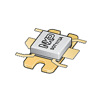
BLF6G10L-40BRN NXP Semiconductors, BLF6G10L-40BRN Datasheet

BLF6G10L-40BRN
Available stocks
Related parts for BLF6G10L-40BRN
BLF6G10L-40BRN Summary of contents
Page 1
... BLF6G10L-40BRN Power LDMOS transistor Rev. 3 — 16 November 2010 1. Product profile 1.1 General description 40 W LDMOS power transistor for base station applications at frequencies from 700 MHz to 1 GHz. Table 1. Typical RF performance at T Mode of operation 2-carrier W-CDMA [1] Test signal: 3GPP test model 1; 64 DPCH; PAR = 7 0.01 % probability on CCDF per carrier; carrier spacing 5 MHz ...
Page 2
... Thermal characteristics thermal resistance from junction to case All information provided in this document is subject to legal disclaimers. Rev. 3 — 16 November 2010 BLF6G10L-40BRN Power LDMOS transistor Simplified outline Graphic symbol [ ...
Page 3
... DPCH 821 MHz; RF performance case Symbol Parameter PAR 7.1 Ruggedness in class-AB operation The BLF6G10L-40BRN is capable of withstanding a load mismatch corresponding to VSWR = through all phases under the following conditions 390 mA BLF6G10L-40BRN Product data sheet Characteristics C per section ...
Page 4
... Figure 1. L gate Definition of transistor impedance 001aam480 80 (1) D (2) (%) (W) L Fig 3. All information provided in this document is subject to legal disclaimers. Rev. 3 — 16 November 2010 BLF6G10L-40BRN Power LDMOS transistor [ (Ω) 5.3 + j2.9 5.6 + j2.3 drain 001aaf059 (dB ...
Page 5
... MHz ( 821 MHz Fig 5. 2-carrier W-CDMA adjacent channel power ratio and peak aspect ratio as function of output power; typical values All information provided in this document is subject to legal disclaimers. Rev. 3 — 16 November 2010 BLF6G10L-40BRN Power LDMOS transistor 001aam483 (1) PAR (2) ACPR 5M ...
Page 6
... All information provided in this document is subject to legal disclaimers. Rev. 3 — 16 November 2010 BLF6G10L-40BRN Power LDMOS transistor C3 C9 BLF6G10L-40BRN Output Circuit RO4350 30 MII NXP C6 BLF6G10L-40BRN Output Circuit RO4350 30 MII NXP C10 014aab232 ...
Page 7
... 9.65 9.65 9.65 9.65 1.14 17.12 9.40 9.40 9.40 9.40 0.89 16.10 0.38 0.38 0.38 0.38 0.045 0.674 0.37 0.37 0.37 0.37 0.035 0.634 References JEDEC JEITA All information provided in this document is subject to legal disclaimers. Rev. 3 — 16 November 2010 BLF6G10L-40BRN Power LDMOS transistor ( 3.00 3.30 1.70 20.45 9.91 15.24 2.69 2.92 1.45 20.19 9.65 0.118 0.130 0.067 ...
Page 8
... The value of VSWR has been corrected. Preliminary data sheet Preliminary data sheet All information provided in this document is subject to legal disclaimers. Rev. 3 — 16 November 2010 BLF6G10L-40BRN Power LDMOS transistor Change notice Supersedes - BLF6G10L-40BRN v.2 has been changed to 390 mA BLF6G10L-40BRN v © NXP B.V. 2010. All rights reserved ...
Page 9
... Export control — This document as well as the item(s) described herein may be subject to export control regulations. Export might require a prior authorization from national authorities. All information provided in this document is subject to legal disclaimers. Rev. 3 — 16 November 2010 BLF6G10L-40BRN Power LDMOS transistor © NXP B.V. 2010. All rights reserved ...
Page 10
... Notice: All referenced brands, product names, service names and trademarks are the property of their respective owners. http://www.nxp.com salesaddresses@nxp.com All information provided in this document is subject to legal disclaimers. Rev. 3 — 16 November 2010 BLF6G10L-40BRN Power LDMOS transistor © NXP B.V. 2010. All rights reserved ...
Page 11
... Please be aware that important notices concerning this document and the product(s) described herein, have been included in section ‘Legal information’. © NXP B.V. 2010. For more information, please visit: http://www.nxp.com For sales office addresses, please send an email to: salesaddresses@nxp.com Document identifier: BLF6G10L-40BRN All rights reserved. Date of release: 16 November 2010 ...


