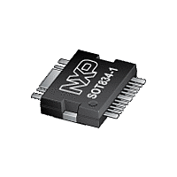
BLM6G22-30 NXP Semiconductors, BLM6G22-30 Datasheet - Page 3

BLM6G22-30
Manufacturer Part Number
BLM6G22-30
Description
30 W LDMOS 2-stage power MMIC for base station applications at frequencies from 2100 MHz to 2200 MHz
Manufacturer
NXP Semiconductors
Datasheet
1.BLM6G22-30.pdf
(14 pages)
Available stocks
Company
Part Number
Manufacturer
Quantity
Price
Company:
Part Number:
BLM6G22-30G
Manufacturer:
ST
Quantity:
23 000
Part Number:
BLM6G22-30G
Manufacturer:
NXP/恩智浦
Quantity:
20 000
NXP Semiconductors
4. Block diagram
5. Limiting values
6. Thermal characteristics
BLM6G22-30_BLM6G22-30G
Product data sheet
Table 4.
In accordance with the Absolute Maximum Rating System (IEC 60134).
Table 5.
[1]
Symbol
V
V
I
I
T
T
Symbol
R
R
D1
D2
Fig 2.
stg
j
DS
GS
th(j-c)1
th(j-c)2
Thermal resistance is determined under specific RF operating conditions.
Block diagram of BLM6G22-30 and BLM6G22-30G
Limiting values
Thermal characteristics
Parameter
drain-source voltage
gate-source voltage
first stage drain current
second stage drain current
storage temperature
junction temperature
Parameter
first stage thermal resistance
from junction to case
second stage thermal resistance
from junction to case
All information provided in this document is subject to legal disclaimers.
RF_INPUT
Rev. 4 — 7 March 2011
V
V
V
DS1
GS1
GS2
BLM6G22-30; BLM6G22-30G
2
6
9
10
COMPENSATED BIAS
TEMPERATURE
W-CDMA 2100 MHz to 2200 MHz power MMIC
Conditions
Conditions
T
2-carrier W-CDMA
T
2-carrier W-CDMA
case
case
= 25 °C; P
= 25 °C; P
14
RF_OUTPUT/V
L
L
001aah621
= 2 W;
= 2 W;
DS2
Min
-
0.5
-
-
−65
-
[1]
[1]
© NXP B.V. 2011. All rights reserved.
Value
3.9
2.1
Max
65
+13
3
9
+150
200
Unit
K/W
K/W
3 of 14
Unit
V
V
A
A
°C
°C


