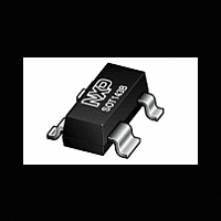
BF1212 NXP Semiconductors, BF1212 Datasheet - Page 2

BF1212
Manufacturer Part Number
BF1212
Description
Enhancement type N-channel Field-Effect Transistor in a plastic SOT143B package
Manufacturer
NXP Semiconductors
Datasheet
1.BF1212.pdf
(16 pages)
Available stocks
Company
Part Number
Manufacturer
Quantity
Price
Company:
Part Number:
BF1212
Manufacturer:
NXP
Quantity:
120 000
Part Number:
BF1212
Manufacturer:
NXP/恩智浦
Quantity:
20 000
Company:
Part Number:
BF1212R
Manufacturer:
NXP
Quantity:
72 000
Part Number:
BF1212R
Manufacturer:
NXP/恩智浦
Quantity:
20 000
Company:
Part Number:
BF1212WR
Manufacturer:
IDT
Quantity:
3 400
Company:
Part Number:
BF1212WR
Manufacturer:
NXP
Quantity:
72 000
Part Number:
BF1212WR
Manufacturer:
NXP/恩智浦
Quantity:
20 000
NXP Semiconductors
FEATURES
Short channel transistor with high forward transfer
Low noise gain controlled amplifier
Excellent low frequency noise performance
Partly internal self-biasing circuit to ensure good
APPLICATIONS
Gain controlled low noise VHF and UHF amplifiers for
DESCRIPTION
Enhancement type N-channel field-effect transistor with
source and substrate interconnected. Integrated diodes
between gates and source protect against excessive input
voltage surges. The BF1212, BF1212R and BF1212WR
are encapsulated in the SOT143B, SOT143R and
SOT343R plastic packages respectively.
QUICK REFERENCE DATA
2003 Nov 14
V
I
P
y
C
C
F
X
T
SYMBOL
D
admittance to input capacitance ratio
cross-modulation performance during AGC and good
DC stabilization.
5 V digital and analog television tuner applications.
j
DS
tot
mod
N-channel dual-gate MOS-FETs
ig1-ss
rss
fs
BF1212R; marking code: LKp
Fig.2 Simplified outline (SOT143R).
handbook, 2 columns
drain-source voltage
drain current
total power dissipation
forward transfer admittance
input capacitance at gate 1
reverse transfer capacitance
noise figure
cross-modulation
junction temperature
3
2
Top view
PARAMETER
MSB035
4
1
f = 800 MHz
input level for k = 1 % at
f = 1 MHz
40 dB AGC
CONDITIONS
2
PINNING
handbook, halfpage
BF1212; marking code: LGp
BF1212WR; marking code: ML
PIN
1
2
3
4
Fig.1 Simplified outline (SOT143B).
Fig.3 Simplified outline (SOT343R).
handbook, 2 columns
28
100
Top view
1
4
MIN.
3
2
Top view
source
drain
gate 2
gate 1
BF1212; BF1212R;
33
1.7
15
1.1
104
TYP.
MSB842
DESCRIPTION
MSB014
4
1
Product specification
3
2
BF1212WR
6
30
180
43
2.2
30
1.8
150
MAX.
V
mA
mW
mS
pF
fF
dB
dBV
C
UNIT


