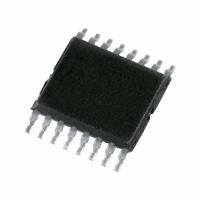
74LVC109PW,118 NXP Semiconductors, 74LVC109PW,118 Datasheet - Page 11

74LVC109PW,118
Manufacturer Part Number
74LVC109PW,118
Description
IC DUAL JK F-F POS-EDGE 16TSSOP
Manufacturer
NXP Semiconductors
Series
74LVCr
Type
JK Typer
Datasheet
1.74LVC109DB118.pdf
(18 pages)
Specifications of 74LVC109PW,118
Output Type
Differential
Package / Case
16-TSSOP
Function
Set(Preset) and Reset
Number Of Elements
2
Number Of Bits Per Element
1
Frequency - Clock
150MHz
Trigger Type
Positive Edge
Current - Output High, Low
24mA, 24mA
Voltage - Supply
2.7 V ~ 3.6 V
Operating Temperature
-40°C ~ 125°C
Mounting Type
Surface Mount
Number Of Circuits
2
Logic Family
LVC
Logic Type
J-K Positive Edge Triggered Flip Flop
Polarity
Inverting/Non-Inverting
Input Type
Single-Ended
Propagation Delay Time
4 ns at 3.3 V
High Level Output Current
- 24 mA
Low Level Output Current
24 mA
Supply Voltage (max)
3.6 V
Maximum Operating Temperature
+ 125 C
Mounting Style
SMD/SMT
Minimum Operating Temperature
- 40 C
Supply Voltage (min)
1.2 V
Lead Free Status / RoHS Status
Lead free / RoHS Compliant
Delay Time - Propagation
-
Lead Free Status / Rohs Status
Lead free / RoHS Compliant
Other names
74LVC109PW-T
74LVC109PW-T
935191070118
74LVC109PW-T
935191070118
Philips Semiconductors
AC WAVEFORMS
2004 Mar 18
handbook, full pagewidth
Dual JK flip-flop with set and reset;
positive-edge trigger
V
V
V
The shaded areas indicate when the input is permitted to change for predictable output performance.
Fig.6
M
M
OL
= 1.5 V at V
= 0.5V
and V
CC
set-up, the nCP to nJ and nK hold times and the maximum clock pulse frequency.
OH
Clock input (nCP) to output (nQ and nQ) propagation delays, the clock pulse width, the nJ and nK to nCP
at V
are typical output voltage drop that occur with the output load.
CC
CC
< 2.7 V.
2.7 V.
nJ, nK input
nCP input
nQ output
nQ output
GND
GND
V OH
V OH
V OL
V OL
V I
V I
V M
t PLH
t su
t h
V M
11
V M
t W
V M
t PHL
1/f max
t PHL
t su
t h
t PLH
MNA860
Product specification
74LVC109


