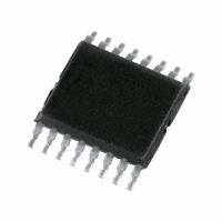
74LVC109PW,118 NXP Semiconductors, 74LVC109PW,118 Datasheet - Page 2

74LVC109PW,118
Manufacturer Part Number
74LVC109PW,118
Description
IC DUAL JK F-F POS-EDGE 16TSSOP
Manufacturer
NXP Semiconductors
Series
74LVCr
Type
JK Typer
Datasheet
1.74LVC109DB118.pdf
(18 pages)
Specifications of 74LVC109PW,118
Output Type
Differential
Package / Case
16-TSSOP
Function
Set(Preset) and Reset
Number Of Elements
2
Number Of Bits Per Element
1
Frequency - Clock
150MHz
Trigger Type
Positive Edge
Current - Output High, Low
24mA, 24mA
Voltage - Supply
2.7 V ~ 3.6 V
Operating Temperature
-40°C ~ 125°C
Mounting Type
Surface Mount
Number Of Circuits
2
Logic Family
LVC
Logic Type
J-K Positive Edge Triggered Flip Flop
Polarity
Inverting/Non-Inverting
Input Type
Single-Ended
Propagation Delay Time
4 ns at 3.3 V
High Level Output Current
- 24 mA
Low Level Output Current
24 mA
Supply Voltage (max)
3.6 V
Maximum Operating Temperature
+ 125 C
Mounting Style
SMD/SMT
Minimum Operating Temperature
- 40 C
Supply Voltage (min)
1.2 V
Lead Free Status / RoHS Status
Lead free / RoHS Compliant
Delay Time - Propagation
-
Lead Free Status / Rohs Status
Lead free / RoHS Compliant
Other names
74LVC109PW-T
74LVC109PW-T
935191070118
74LVC109PW-T
935191070118
Philips Semiconductors
FEATURES
QUICK REFERENCE DATA
GND = 0 V; T
Notes
1. C
2. The condition is V
2004 Mar 18
t
f
C
C
PHL
max
SYMBOL
5 V tolerant inputs for interfacing with 5 V logic
Wide supply voltage range from 1.2 to 3.6 V
CMOS low power consumption
Direct interface with TTL levels
Inputs accept voltages up to 5.5 V
Complies with JEDEC standard no. 8-1A
ESD protection:
HBM EIA/JESD22-A114-A exceeds 2000 V
MM EIA/JESD22-A115-A exceeds 200 V.
Specified from 40 to +85 C and 40 to +125 C.
I
PD
Dual JK flip-flop with set and reset;
positive-edge trigger
P
f
f
C
V
N = total load switching outputs;
i
o
/t
(C
D
CC
PD
= input frequency in MHz;
L
PLH
= output frequency in MHz;
= output load capacitance in pF;
= C
L
is used to determine the dynamic power dissipation (P
= supply voltage in Volts;
PD
V
CC
amb
propagation delay nCP to nQ
and nCP to nQ
propagation delay nSD to nQ
and nRD to nQ
propagation delay nSD to nQ
and nRD to nQ
maximum clock frequency
input capacitance
power dissipation capacitance per
flip-flop
2
V
CC
= 25 C; t
f
o
2
) = sum of the outputs.
I
f
= GND to V
i
PARAMETER
N + (C
r
= t
f
2.5 ns.
L
CC
.
V
CC
2
f
o
) where:
C
C
C
C
notes 1 and 2
L
L
L
L
= 50 pF; R
= 50 pF; R
= 50 pF; R
= 50 pF; R
2
DESCRIPTION
The 74LVC109A is a high-performance, low-voltage,
Si-gate CMOS device, superior to most advanced CMOS
compatible TTL families.
The 74LVC109A is a dual positive edge triggered
JK flip-flop featuring individual J and K inputs, clock (CP)
inputs, set (SD) and reset (RD) inputs and complementary
Q and Q outputs.
The set and reset are asynchronous active LOW inputs
and operate independently of the clock input.
The J and K inputs control the state changes of the
flip-flops as described in the mode select function table.
The J and K inputs must be stable one set-up time prior to
the LOW-to-HIGH clock transition for predictable
operation. The JK design allows operation as a D-type
flip-flop by tying the J and K inputs together.
Schmitt-trigger action in the clock input makes the circuit
highly tolerant to slower clock rise and fall times.
D
CONDITIONS
in W).
L
L
L
L
= 500 ; V
= 500 ; V
= 500 ; V
= 500 ; V
CC
CC
CC
CC
= 3.3 V
= 3.3 V
= 3.3 V
= 3.3 V
3.8
3.2
3.5
330
5.0
23
TYPICAL
Product specification
74LVC109
ns
ns
ns
MHz
pF
pF
UNIT


