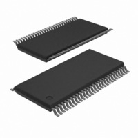
74ALVCH16841DGG,11 NXP Semiconductors, 74ALVCH16841DGG,11 Datasheet - Page 4

74ALVCH16841DGG,11
Manufacturer Part Number
74ALVCH16841DGG,11
Description
IC 20BIT BUS INTRFC D 56TSSOP
Manufacturer
NXP Semiconductors
Series
74ALVCHr
Type
D-Typer
Datasheet
1.74ALVCH16841DGG11.pdf
(10 pages)
Specifications of 74ALVCH16841DGG,11
Logic Type
D-Type Transparent Latch
Package / Case
56-TSSOP
Circuit
10:10
Output Type
Tri-State
Voltage - Supply
2.3 V ~ 3.6 V
Independent Circuits
2
Delay Time - Propagation
2.5ns
Current - Output High, Low
24mA, 24mA
Operating Temperature
-40°C ~ 85°C
Mounting Type
Surface Mount
Number Of Circuits
2
Logic Family
ALVC
Polarity
Non-Inverting
Input Bias Current (max)
0.2 uA
High Level Output Current
- 24 mA
Low Level Output Current
24 mA
Propagation Delay Time
2.4 ns at 3.3 V
Supply Voltage (max)
3.6 V
Supply Voltage (min)
2.3 V
Maximum Operating Temperature
+ 85 C
Minimum Operating Temperature
- 40 C
Mounting Style
SMD/SMT
Number Of Bits
20
Number Of Elements
2
Latch Mode
Transparent
Technology
CMOS
Package Type
TSSOP
Operating Supply Voltage (typ)
2.5/3.3V
Operating Supply Voltage (min)
2.3V
Operating Supply Voltage (max)
3.6V
Operating Temp Range
-40C to 85C
Operating Temperature Classification
Industrial
Mounting
Surface Mount
Pin Count
56
Lead Free Status / RoHS Status
Lead free / RoHS Compliant
Lead Free Status / RoHS Status
Lead free / RoHS Compliant, Lead free / RoHS Compliant
Other names
74ALVCH16841DG-T
74ALVCH16841DG-T
935259090118
74ALVCH16841DG-T
935259090118
1. The input and output voltage ratings may be exceeded if the input and output current ratings are observed.
Philips Semiconductors
BUS HOLD CIRCUIT
RECOMMENDED OPERATING CONDITIONS
ABSOLUTE MAXIMUM RATINGS
In accordance with the Absolute Maximum Rating System (IEC 134)
Voltages are referenced to GND (ground = 0V)
NOTE:
1998 Jul 27
SYMBOL
20-bit bus interface D-type latch (3-State)
SYMBOL
I
GND
T
V
V
t
P
V
amb
r
V
V
T
I
CC
CC
, t
V
I
TOT
Data Input
O
V
V
OK
I
CC
IK
stg
I
O
O
, I
f
I
I
CC
DC supply voltage 2.5V range (for max. speed
performance @ 30 pF output load)
DC supply voltage 3.3V range (for max. speed
performance @ 50 pF output load)
DC Input voltage range
DC output voltage range
Operating free-air temperature range
Input rise and fall times
DC supply voltage
DC input diode current
DC input voltage
DC in ut voltage
DC output diode current
DC output voltage
DC output source or sink current
DC V
Storage temperature range
Power dissipation per package
–plastic medium-shrink (SSOP)
–plastic thin-medium-shrink (TSSOP)
V
CC
CC
or GND current
PARAMETER
PARAMETER
To internal circuit
SW00044
V
For control pins
For data inputs
V
Note 1
V
For temperature range: –40 to +125 C
above +55 C derate linearly with 11.3 mW/K
above +55 C derate linearly with 8 mW/K
I
O
O
t0
uV
= 0 to V
CC
or V
CC
4
V
V
O
1
CC
CC
1
CONDITIONS
CONDITIONS
t 0
= 2.3 to 3.0V
= 3.0 to 3.6V
MIN
–40
2.3
3.0
0
0
0
0
–0.5 to V
–0.5 to V
–0.5 to +4.6
–0.5 to +4.6
–65 to +150
74ALVCH16841
RATING
"100
"50
"50
–50
850
600
MAX
V
V
+85
2.7
3.6
CC
CC
20
10
CC
CC
+0.5
+0.5
Product specification
UNIT
ns/V
UNIT
mW
mA
mA
mA
mA
V
V
V
V
C
V
V
V
V
C


