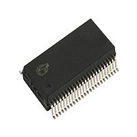
CY14B101LA-SP45XI Cypress Semiconductor Corp, CY14B101LA-SP45XI Datasheet - Page 24

CY14B101LA-SP45XI
Manufacturer Part Number
CY14B101LA-SP45XI
Description
IC NVSRAM 1MBIT 45NS 48SSOP
Manufacturer
Cypress Semiconductor Corp
Type
NVSRAMr
Datasheet
1.CY14B101LA-SP45XI.pdf
(26 pages)
Specifications of CY14B101LA-SP45XI
Format - Memory
RAM
Memory Type
NVSRAM (Non-Volatile SRAM)
Memory Size
1M (128K x 8)
Speed
45ns
Interface
Parallel
Voltage - Supply
2.7 V ~ 3.6 V
Operating Temperature
-40°C ~ 85°C
Package / Case
*
Word Size
8b
Organization
128Kx8
Density
1Mb
Interface Type
Parallel
Access Time (max)
45ns
Package Type
SSOP
Operating Temperature Classification
Industrial
Operating Supply Voltage (max)
3.6V
Operating Supply Voltage (min)
2.7V
Operating Temp Range
-40C to 85C
Pin Count
48
Mounting
Surface Mount
Supply Current
52mA
Memory Configuration
128K X 8
Access Time
45ns
Supply Voltage Range
2.7V To 3.6V
Memory Case Style
SSOP
No. Of Pins
48
Operating Temperature Range
-40°C To +85°C
Rohs Compliant
Yes
Lead Free Status / RoHS Status
Lead free / RoHS Compliant
Available stocks
Company
Part Number
Manufacturer
Quantity
Price
Company:
Part Number:
CY14B101LA-SP45XI
Manufacturer:
CY
Quantity:
35 792
Part Number:
CY14B101LA-SP45XI
Manufacturer:
CYPRESS/赛普拉斯
Quantity:
20 000
Document History Page
Document #: 001-42879 Rev. *K
Document Title: CY14B101LA, CY14B101NA 1-Mbit (128 K × 8/64 K × 16) nvSRAM
Document Number: 001-42879
Rev.
*A
*B
**
ECN No.
2050747
2607447
2654484
GVCH/PYRS
GVCH/AESA
UNC/PYRS
Change
Orig. of
Submission
01/31/08
02/05/09
11/14/08
Date
New Datasheet
Changed the datasheet from Advance information to Preliminary
Removed 15 ns access speed
Updated “Features”
Updated Logic block diagram
Added footnote 1 2, 3 and 7
Pin definition: Updated WE, HSB and NC pin description
Page 4: Updated SRAM READ, SRAM WRITE, AutoStore operation description
Updated Figure 4
Page 4: Updated Hardware store operation and Hardware RECALL (Pow-
erup)description
Page 4: Updated Software store and software recall description
Footnote 1 and 11 referenced for Mode selection Table
Added footnote 11
Updated footnote 9 and 10
Page 6: updated Data protection description
Maximum Ratings:Added Max. Accumulated storage time
Changed Output short circuit current parameter name to DC output current
Changed I
Changed I
Changed I
Changed I
Added I
Updated I
Changed V
Added V
Updated footnote 12 and 13
Added footnote 14
Added Data retention and Endurance Table
Added thermal resistance value to 48-pin FBGA and 44-pin TSOP II packages
Updated Input Rise and Fall time in AC test Conditions
Referenced footnote 17 to t
Updated All switching waveforms
Updated footnote 17
Added footnote 20
Added Figure 10 (SRAM WRITE CYCLE:BHE and BLE controlled)
Changed t
Updated t
Added V
Updated footnote 24
Added footnote 26 and 27
Software controlled STORE/RECALL Table: Changed t
Changed t
Changed t
Added Figure 13
Added t
Changed t
Updated t
Added truth table for SRAM operations
Updated ordering information and part numbering nomenclature
Referenced Note 15 to parameters t
Updated Figure 12
IX
DHSB
CAP
HDIS
CC1,
DELAY
SS
for HSB
CC2
CC3
CC4
SB
STORE
GHAX
HA
HLHX
CAP
from 70 us to 100 us
voltage max value to 180uF
, t
value from 1 ns to 0 ns
parameter
from 3 mA to 5 mA
I
from 6 mA to 10 mA
from 15 mA to 35 mA
from 6 mA to 5 mA
HHHD
CC3,
voltage min value from 68 uF to 61 uF
to t
to t
value
max value from 12.5 ms to 8 ms
PHSB
HA
I
SB
and t
and I
LZHSB
Description of Change
OHA
OZ
Test conditions
parameter
parameters
LZCE
, t
HZCE
, t
LZOE,
AS
t
HZOE,
CY14B101NA
CY14B101LA
to t
SA
t
LZWE
Page 24 of 26
and t
HZWE
[+] Feedback


