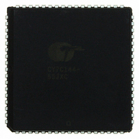
CY7C144-55JXC Cypress Semiconductor Corp, CY7C144-55JXC Datasheet - Page 12

CY7C144-55JXC
Manufacturer Part Number
CY7C144-55JXC
Description
IC SRAM 64KBIT 55NS 68PLCC
Manufacturer
Cypress Semiconductor Corp
Type
Asynchronousr
Datasheet
1.CY7C144-55AXC.pdf
(23 pages)
Specifications of CY7C144-55JXC
Memory Size
64K (8K x 8)
Package / Case
68-PLCC
Format - Memory
RAM
Memory Type
SRAM - Dual Port, Asynchronous
Speed
55ns
Interface
Parallel
Voltage - Supply
4.5 V ~ 5.5 V
Operating Temperature
0°C ~ 70°C
Access Time
55 ns
Supply Voltage (max)
5.5 V
Supply Voltage (min)
4.5 V
Maximum Operating Current
160 mA
Maximum Operating Temperature
+ 70 C
Minimum Operating Temperature
0 C
Mounting Style
SMD/SMT
Number Of Ports
2
Operating Supply Voltage
5 V
Lead Free Status / RoHS Status
Lead free / RoHS Compliant
Lead Free Status / RoHS Status
Lead free / RoHS Compliant, Lead free / RoHS Compliant
Other names
428-2155
CY7C144-55JXC
CY7C144-55JXC
Available stocks
Company
Part Number
Manufacturer
Quantity
Price
Company:
Part Number:
CY7C144-55JXC
Manufacturer:
Cypress Semiconductor Corp
Quantity:
10 000
Company:
Part Number:
CY7C144-55JXCT
Manufacturer:
CYPRESS10
Quantity:
2 950
Company:
Part Number:
CY7C144-55JXCT
Manufacturer:
Cypress Semiconductor Corp
Quantity:
10 000
Switching Waveforms
Notes
Document #: 38-06034 Rev. *H
19. The internal write time of the memory is defined by the overlap of CE or SEM LOW and R/W LOW. Both signals must be LOW to initiate a write, and either signal can
20. If OE is LOW during a R/W controlled write cycle, the write pulse width must be the larger of t
21. R/W must be HIGH during all address transitions.
22. Data I/O pins enter high impedance when OE is held LOW during write.
Data Out
terminate a write by going HIGH. The data input set-up and hold timing should be referenced to the rising edge of the signal that terminates the write.
placed on the bus for the required t
be as short as the specified t
SEM OR CE
Address
SEM OR CE
Data Out
Data In
Address
Data In
R/W
OE
R/W
Figure 9. Write Cycle No. 2: R/W Three-State Data I/Os (Either Port)
Figure 8. Write Cycle No. 1: OE Three-State Data I/Os (Either Port)
PWE
t
SA
.
SD
. If OE is HIGH during a R/W controlled write cycle (as in this example), this requirement does not apply and the write pulse can
(continued)
t
SA
t
HZOE
t
SCE
t
SCE
t
AW
t
AW
High Impedance
t
HZWE
t
WC
t
WC
t
PWE
t
PWE
PWE
t
SD
Data Valid
t
SD
or (t
High Impedance
Data Valid
HZWE
+ t
SD
) to allow the I/O drivers to turn off and data to be
t
HD
t
t
HD
LZWE
t
[19, 20, 21]
HA
t
[19, 21, 22]
LZOE
t
HA
CY7C144 CY7C145
Page 12 of 23
[+] Feedback


