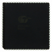
CY7C144-55JXC Cypress Semiconductor Corp, CY7C144-55JXC Datasheet - Page 8

CY7C144-55JXC
Manufacturer Part Number
CY7C144-55JXC
Description
IC SRAM 64KBIT 55NS 68PLCC
Manufacturer
Cypress Semiconductor Corp
Type
Asynchronousr
Datasheet
1.CY7C144-55AXC.pdf
(23 pages)
Specifications of CY7C144-55JXC
Memory Size
64K (8K x 8)
Package / Case
68-PLCC
Format - Memory
RAM
Memory Type
SRAM - Dual Port, Asynchronous
Speed
55ns
Interface
Parallel
Voltage - Supply
4.5 V ~ 5.5 V
Operating Temperature
0°C ~ 70°C
Access Time
55 ns
Supply Voltage (max)
5.5 V
Supply Voltage (min)
4.5 V
Maximum Operating Current
160 mA
Maximum Operating Temperature
+ 70 C
Minimum Operating Temperature
0 C
Mounting Style
SMD/SMT
Number Of Ports
2
Operating Supply Voltage
5 V
Lead Free Status / RoHS Status
Lead free / RoHS Compliant
Lead Free Status / RoHS Status
Lead free / RoHS Compliant, Lead free / RoHS Compliant
Other names
428-2155
CY7C144-55JXC
CY7C144-55JXC
Available stocks
Company
Part Number
Manufacturer
Quantity
Price
Company:
Part Number:
CY7C144-55JXC
Manufacturer:
Cypress Semiconductor Corp
Quantity:
10 000
Company:
Part Number:
CY7C144-55JXCT
Manufacturer:
CYPRESS10
Quantity:
2 950
Company:
Part Number:
CY7C144-55JXCT
Manufacturer:
Cypress Semiconductor Corp
Quantity:
10 000
Electrical Characteristics
Over the Operating Range (continued)
Capacitance
Tested initially and after any design or process changes that may affect these parameters.
Note
Document #: 38-06034 Rev. *H
V
V
V
V
I
I
I
I
I
I
I
C
C
6. f
IX
OZ
CC
SB1
SB2
SB3
SB4
OH
OL
IH
IL
IN
OUT
Parameter
Parameter
Output
Output
MAX
C = 30 pF
= 1/t
(a) Normal Load (Load1)
RC
Load (Load 2)
= All inputs cycling at f = 1/t
Input capacitance
Output capacitance
Output HIGH voltage
Output LOW voltage
Input HIGH voltage
Input LOW voltage
Input leakage vurrent
Output leakage current Outputs disabled, GND < V
Operating current
Standby current
(Both ports TTL levels)
Standby current
(One port TTL level)
Standby current
(Both ports CMOS
levels)
Standby current
(One port CMOS level)
C = 30 pF
Description
Description
5 V
R1 = 893
R2 = 347
RC
(except output enable). f = 0 means no address or control lines change. This applies only to inputs at CMOS level standby I
GND < V
V
T
V
V
V
Outputs disabled
CE
f = f
CE
f = f
Both ports
CE and CE
V
One port
CE
V
V
GND
3.0 V
A
CC
CC
CC
IN
IN
IN
CC
Figure 4. AC Test Loads and Waveforms
= 25 C, f = 1 MHz,
L
L
L
MAX
MAX
> V
> V
< 0.2 V, Active Port outputs, f = f
3 ns
= Min., I
= Min., I
= Max., I
and CE
or CE
or CE
= 5.0 V
CC
CC
Output
[6]
[6]
I
10%
< V
R
– 0.2 V or V
R
– 0.2 V or
C = 30pF
R
(b) Th évenin Equivalent (Load 1)
R
> V
> V
Test Conditions
OH
OL
> V
OUT
CC
> V
= 4.0 mA
IH
CC
= 4.0 mA
CC
All Input Pulses
IH
,
= 0 mA
90%
– 0.2 V,
,
– 0.2 V,
Test Conditions
IN
R
TH
< 0.2 V, f = 0
= 250
O
< V
CC
V
MAX
90%
TH
[6]
10%
= 1.4 V
[6]
3 ns
Commercial
Industrial
Commercial
Industrial
Commercial
Industrial
Commercial
Industrial
Commercial
Industrial
Output
C = 5 pF
Max
(c) Three-State Delay (Load 3)
10
15
CY7C144 CY7C145
Min
10
10
2.4
2.2
7C144-55
Max
+10
+10
160
180
100
110
100
0.4
0.8
5 V
30
40
15
30
90
Page 8 of 23
R1 = 893
R = 347
Unit
pF
pF
Unit
mA
mA
mA
mA
mA
A
A
V
V
V
V
SB3
[+] Feedback


