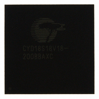
CYD18S18V18-200BBAXC Cypress Semiconductor Corp, CYD18S18V18-200BBAXC Datasheet - Page 13

CYD18S18V18-200BBAXC
Manufacturer Part Number
CYD18S18V18-200BBAXC
Description
IC SRAM 18MBIT 200MHZ 256LFBGA
Manufacturer
Cypress Semiconductor Corp
Datasheet
1.CYD02S36V18-167BBC.pdf
(52 pages)
Specifications of CYD18S18V18-200BBAXC
Memory Size
18M (1M x 18)
Format - Memory
RAM
Memory Type
SRAM - Dual Port, Synchronous
Speed
200MHz
Interface
Parallel
Voltage - Supply
1.42 V ~ 1.58 V, 1.7 V ~ 1.9 V
Operating Temperature
0°C ~ 70°C
Package / Case
256-LFBGA
Memory Configuration
1M X 18
Clock Frequency
77MHz
Access Time
3.3ns
Supply Voltage Range
1.42V To 1.58V, 1.7V To 1.9V
Memory Case Style
BGA
No. Of Pins
256
Rohs Compliant
Yes
Lead Free Status / RoHS Status
Lead free / RoHS Compliant
Other names
428-2036
Available stocks
Company
Part Number
Manufacturer
Quantity
Price
Company:
Part Number:
CYD18S18V18-200BBAXC
Manufacturer:
Cypress Semiconductor Corp
Quantity:
10 000
Address Counter and Mask Register Operations
Each port of the FullFlex family contains a programmable burst
address counter. The burst counter contains four registers: a
counter register, a mask register, a mirror register, and a busy
address register.
The counter register contains the address used to access the
RAM array. It is changed only by the master reset (MRST),
counter reset, counter load, retransmit, and counter increment
operations.
The mask register value affects the counter increment and
counter reset operations by preventing the corresponding bits of
the counter register from changing. It also affects the counter
interrupt output (CNTINT). The mask register is only changed by
mask reset, mask load, and MRST. The mask load operation
loads the value of the address bus into the mask register. The
mask register defines the counting range of the counter register.
The mask register is divided into two or three consecutive
regions. Zero or more 0s define the masked region and one or
more 1s define the unmasked portion of the counter register. The
counter register may be divided up to three regions. The region
containing the least significant bits must be no more than two 0s.
Bits one and zero may be 10 respectively, masking the least
significant counter bit and causing the counter to increment by
two instead of one. If bits one and zero are 00, the two least
significant bits are masked and the counter increments by four
instead of one. For example, in the case of a 256 K × 72
configuration, a mask register value of 003FC divides the mask
register into three regions. With bit 0 being the least significant
bit and bit 17 being the most significant bit, the two least
significant bits are masked, the next eight bits are unmasked,
and the remaining bits are masked.
The mirror register reloads a counter register on retransmit
operations (see
Counter Interrupt on page 15
the counter register is stored in the mirror register. The mirror
register is only changed by master reset (MRST), counter reset,
and counter load.
Table 7 on page 14
and the required input control signals. All signals except MRST
are synchronized to the ports clock.
Note
Document Number: 38-06082 Rev. *J
27. The CYD36S18V18 device has 21 address bits. The CYD36S36V18 and CYD18S18V18 devices have 20 address bits. The CYD36S72V18, CYD18S36V18, and
CYD09S18V18 devices have 19 address bits. The CYD18S72V18, CYD09S36V18, and CYD04S18V18 devices have 18 address bits. The CYD09S72V18 and
CYD04S36V18 devices have 17 address bits. The CYD04S72V18 and CYD02S36V18 have 16 address bits.
Retransmit on page
summarizes the operations of these registers
below). The last value loaded into
15) and wrap functions (see
[27]
Counter Load Operation
For both non-burst and burst read or write accesses, the external
address is loaded through counter load operation as shown in
Table 7. The address counter and mirror registers are loaded
with the address value presented on the address lines. This
value ranges from 0 to 1FFFFF.
Mask Load Operation
The mask register is loaded with the address value presented on
the address bus. This value ranges from 0 to 1FFFFF though not
all values permit correct increment operations. Permitted values
are in the form of 2
segmented up to three regions. From the most significant bit to
the least significant bit, permitted values have zero or more 0s,
one or more 1s, and the least significant two bits are 11, 10, or
00. Thus 1FFFFE, 07FFFF, and 003FFC are permitted values
but 02FFFF, 003FFA, and 07FFE4 are not.
Counter Readback Operation
The internal value of the counter register is read out on the
address lines. The address is valid t
of latency cycles configured by FTSEL. The data bus (DQ) is
tri-stated on the cycle that the address is presented on the
address lines.
logic.
Mask Readback Operation
The internal value of the mask register is read out on the address
lines. The address is valid t
latency cycles configured by FTSEL. The data bus (DQ) is
tri-stated on the cycle that the address is presented on the
address lines.
operation.
Counter Reset Operation
All unmasked bits of the counter and mirror registers are reset to
‘0’. All masked bits remain unchanged. A mask reset followed by
a counter reset resets the counter and mirror registers to 00000.
Mask Reset Operation
The mask register is reset to all 1s, that unmasks every bit of the
burst counter.
Figure 7
Figure 7
n
–1, 2
on page 16 shows a block diagram of this
on page 16 shows a block diagram of the
n
–2, or 2
[27]
[27]
CA
n
–4. The counter register is only
after the selected number of
CA
after the selected number
Page 13 of 52
FullFlex
[+] Feedback


