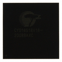
CYD18S18V18-200BBAXC Cypress Semiconductor Corp, CYD18S18V18-200BBAXC Datasheet - Page 26

CYD18S18V18-200BBAXC
Manufacturer Part Number
CYD18S18V18-200BBAXC
Description
IC SRAM 18MBIT 200MHZ 256LFBGA
Manufacturer
Cypress Semiconductor Corp
Datasheet
1.CYD02S36V18-167BBC.pdf
(52 pages)
Specifications of CYD18S18V18-200BBAXC
Memory Size
18M (1M x 18)
Format - Memory
RAM
Memory Type
SRAM - Dual Port, Synchronous
Speed
200MHz
Interface
Parallel
Voltage - Supply
1.42 V ~ 1.58 V, 1.7 V ~ 1.9 V
Operating Temperature
0°C ~ 70°C
Package / Case
256-LFBGA
Memory Configuration
1M X 18
Clock Frequency
77MHz
Access Time
3.3ns
Supply Voltage Range
1.42V To 1.58V, 1.7V To 1.9V
Memory Case Style
BGA
No. Of Pins
256
Rohs Compliant
Yes
Lead Free Status / RoHS Status
Lead free / RoHS Compliant
Other names
428-2036
Available stocks
Company
Part Number
Manufacturer
Quantity
Price
Company:
Part Number:
CYD18S18V18-200BBAXC
Manufacturer:
Cypress Semiconductor Corp
Quantity:
10 000
Switching Characteristics
Over the Operating Range
Table 14. SDR Mode
Notes
Document Number: 38-06082 Rev. *J
f
(P
f
THROUGH
t
(P
t
THROUGH
t
t
t
t
t
t
t
Table 13. SDR Mode, Signals Affected by DLL
t
t
t
t
MAX
MAX
CYC
CYC
CKD
SD
HD
SAC
HAC
OE
OLZ
43. Parameters specified with the load capacitance in
44. For the x18 devices, add 200 ps to this parameter in
45. Test conditions assume a signal transition time of 2 V/ns.
46. Add 300 ps to this timing for 36M devices.
47. Add 15% to this parameter if a VCORE of 1.5 V is used.
48. This parameter assumes input clock cycle to cycle jitter of ± 0ps.
CD2
CCQ
CKHZ2
CKLZ2
Parameter
Parameter
IPELINED
IPELINED
[46]
[43]
[48]
[46]
[48]
(F
(F
[43, 48]
[43, 48]
LOW X
LOW
)
)
)
)
Maximum operating frequency for pipelined mode
Maximum operating frequency for flow through
mode
C clock cycle time for pipelined mode
C clock cycle time for flow through mode
C clock duty time
Data input setup time to
C rise
Data input hold time after C rise
Address and control
input setup time to C
rise
Address and control input hold time after C rise
Output enable to data valid
OE to low Z
C rise to DQ valid for pipelined
mode
C rise to CQ rise
C rise to DQ output high Z in
pipelined mode
C rise to DQ output low Z in
pipelined mode
Description
Description
HSTL
1.8 V LVCMOS
2.5 V LVCMOS 3.3 V
LVTTL
HSTL
1.8 V L VCMOS
2.5 V LVCMOS 3.3 V
LVTTL
Figure 9
Table
14.
and
1.00
1.00
1.00
Min
–
Figure
–200
3.30
10.
[44, 47]
[44, 47]
Max
3.30
3.30
–
[47]
DLL ON (LOWSPD=1)
[44, 47]
[44, 47]
[44, 46,
[44, 46,
13.00
0.50
1.00
1.00
1.00
5.00
1.50
1.75
1.50
1.75
1.00
Min
Min
100
[47]
[47]
0.5
45
47]
47]
–
–
–
–167
–200
4.00
[44, 47]
[44, 47]
10.00
[44,47]
Max
4.00
4.00
Max
4.40
200
77
55
–
–
–
–
–
–
–
–
–
[47]
[45]
[44, 47]
[44, 47]
[44, 46,
[44, 46,
15.00
1.00
1.00
1.00
6.00
1.70
1.95
1.70
1.95
0.60
1.00
Min
Min
100
0.5
[47]
[47]
45
47]
47]
–
–
–
–133
–167
4.50
[44, 47]
[44, 47]
10.00
[44,47]
Max
4.50
4.50
Max
66.7
5.00
167
55
–
–
–
–
–
–
–
–
[47]
[44, 47]
[44, 47]
[44, 46,
[44, 46,
18.00
1.00
1.00
1.00
7.00
1.80
2.05
1.80
2.05
0.70
1.00
Min
Min
100
(LOWSPD=0)
[47]
[47]
0.5
45
47]
47]
–
–
–
DLL OFF
–133
[45]
6.00
[44, 47]
[44, 47]
10.00
[44,47]
Max
6.00
6.00
Max
55.6
5.50
133
55
Page 26 of 52
–
–
–
–
–
–
–
–
–
FullFlex
[47]
MHz
MHz
Unit
Unit
ns
ns
ns
ns
ns
ns
ns
ns
ns
ns
ns
ns
ns
ns
%
[+] Feedback


