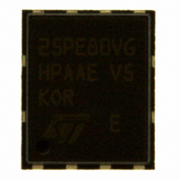
M25PE80-VMP6TG NUMONYX, M25PE80-VMP6TG Datasheet - Page 37

M25PE80-VMP6TG
Manufacturer Part Number
M25PE80-VMP6TG
Description
IC FLASH 8MBIT 75MHZ 8VFQFPN
Manufacturer
NUMONYX
Series
Forté™r
Datasheet
1.M25PE80-VMN6TP.pdf
(66 pages)
Specifications of M25PE80-VMP6TG
Format - Memory
FLASH
Memory Type
FLASH
Memory Size
8M (1M x 8)
Speed
75MHz
Interface
SPI, 3-Wire Serial
Voltage - Supply
2.7 V ~ 3.6 V
Operating Temperature
-40°C ~ 85°C
Package / Case
8-VFQFN, 8-VFQFPN
Cell Type
NOR
Density
8Mb
Access Time (max)
8ns
Interface Type
Serial (SPI)
Boot Type
Not Required
Address Bus
1b
Operating Supply Voltage (typ)
3.3V
Operating Temp Range
-40C to 85C
Package Type
VFQFPN
Program/erase Volt (typ)
2.7 to 3.6V
Sync/async
Synchronous
Operating Temperature Classification
Industrial
Operating Supply Voltage (min)
2.7V
Operating Supply Voltage (max)
3.6V
Word Size
8b
Number Of Words
1M
Supply Current
8mA
Mounting
Surface Mount
Pin Count
8
Lead Free Status / RoHS Status
Lead free / RoHS Compliant
Other names
M25PE80-VMP6TG
M25PE80-VMP6TGTR
M25PE80-VMP6TGTR
Available stocks
Company
Part Number
Manufacturer
Quantity
Price
Company:
Part Number:
M25PE80-VMP6TG
Manufacturer:
Micron Technology Inc
Quantity:
10 000
Part Number:
M25PE80-VMP6TG
Manufacturer:
ST
Quantity:
20 000
M25PE80
6.11
Write to lock register (WRLR)
The write to lock register (WRLR) instruction allows bits to be changed in the lock registers.
Before it can be accepted, a Write Enable (WREN) instruction must previously have been
executed. After the write enable (WREN) instruction has been decoded, the device sets the
write enable latch (WEL).
The write to lock register (WRLR) instruction is entered by driving Chip Select (S) Low,
followed by the instruction code, three address bytes (pointing to any address in the targeted
sector and one data byte on serial data input (D). The instruction sequence is shown in
Figure
latched in, otherwise the write to lock register (WRLR) instruction is not executed.
Lock register bits are volatile, and therefore do not require time to be written. When the write
to lock register (WRLR) instruction has been successfully executed, the write enable latch
(WEL) bit is reset after a delay time less than t
Any write to lock register (WRLR) instruction, while an erase, program or write cycle is in
progress, is rejected without having any effects on the cycle that is in progress.
Figure 17. Write to lock register (WRLR) instruction sequence
Table 12.
1. The table rows in gray are true for products processed in the T7Y process only (see
All sectors in T9HX process
All sectors except for sector 0
and sector 15 in T7Y process
S
C
D
page
17. Chip Select (S) must be driven High after the eighth bit of the data byte has been
6).
Sector
Lock register in
0
1
2
Instruction
3
4
5
(1)
b7-b2
6
Bit
b1
b0
7
MSB
23
8
Sector lock down bit value (refer to
Sector write lock bit value (refer to
22 21
9 10
24-bit address
SHSL
3
28 29 30 31 32 33 34 35
2
minimum value.
1
0
MSB
7
Value
6
‘0’
Lock register
5
4
Table
in
Table
3
Important note on
36 37 38
2
11)
11)
1
Instructions
0
39
AI10784
37/66


