M27C512-90F6 STMicroelectronics, M27C512-90F6 Datasheet - Page 11
M27C512-90F6
Manufacturer Part Number
M27C512-90F6
Description
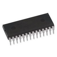
IC EPROM 512KBIT 90NS 28CDIP
Manufacturer
STMicroelectronics
Specifications of M27C512-90F6
Format - Memory
EPROMs
Memory Type
UV EPROM
Memory Size
512K (64K x 8)
Speed
90ns
Interface
Parallel
Voltage - Supply
4.5 V ~ 5.5 V
Operating Temperature
-40°C ~ 85°C
Package / Case
28-CDIP (0.600", 15.24mm) Window
Memory Configuration
64K X 8
Access Time
90ns
Supply Voltage Range
4.5V To 5V
Memory Case Style
DIP
No. Of Pins
28
Rohs Compliant
Yes
Lead Free Status / RoHS Status
Lead free / RoHS Compliant
Available stocks
Company
Part Number
Manufacturer
Quantity
Price
Company:

Part Number:
M27C512-90F6
Manufacturer:
ST
Quantity:
1 450
Company:
Part Number:
M27C512-90F6
Manufacturer:
ST
Quantity:
5 704
Company:
Part Number:
M27C512-90F6
Manufacturer:
ST
Quantity:
5 704
Part Number:
M27C512-90F6
Manufacturer:
ST
Quantity:
20 000
Company:
Part Number:
M27C512-90F6L
Manufacturer:
AD
Quantity:
196
Part Number:
M27C512-90F6L
Manufacturer:
ST
Quantity:
20 000


Table 7. Read Mode DC Characteristics
Note: 1. V
Table 8. Read Mode AC Characteristics
Note: 1. V
t
t
Symbol
GHQZ
Symbol
EHQZ
t
t
t
V
t
GLQV
AXQX
AVQV
ELQV
I
I
V
V
I
IH
I
CC1
CC2
I
V
I
LO
CC
PP
OH
LI
OL
2. Maximum DC voltage on Output is V
2. Sampled only, not 100% tested.
3. Speed obtained with High Speed AC measurement conditions.
IL
(2)
(2)
(2)
CC
CC
t
must be applied simultaneously with or before V
must be applied simultaneously with or before V
ACC
t
t
Input Leakage Current
Output Leakage Current
Supply Current
Supply Current (Standby) TTL
Supply Current (Standby) CMOS
Program Current
Input Low Voltage
Input High Voltage
Output Low Voltage
Output High Voltage TTL
Output High Voltage CMOS
Alt
t
t
t
CE
OE
OH
DF
DF
Address Valid to
Output Valid
Chip Enable Low to
Output Valid
Output Enable Low
to Output Valid
Chip Enable High
to Output Hi-Z
Output Enable
High to Output Hi-Z
Address Transition
to Output Transition
Parameter
Parameter
CC
Test Condition
E = V
E = V
+0.5V.
G = V
G = V
E = V
E = V
IL
IL
, G = V
, G = V
IL
IL
IL
IL
PP
PP
I
and removed simultaneously or after V
IL
IL
and removed simultaneously or after V
OUT
(1)
Test Condition
0V
E = V
E > V
0V
I
OH
I
= 0mA, f = 5MHz
I
OL
V
OH
Min
0
0
0
PP
E = V
V
-45
= –100µA
IL
= 2.1mA
V
CC
OUT
= –1mA
, G = V
IN
= V
(3)
Max
– 0.2V
IH
45
45
25
25
25
CC
V
V
CC
CC
IL
(1)
,
Min
0
0
0
-60
Max
M27C512
60
60
30
25
25
V
CC
Min
–0.3
0
0
0
Min
PP
PP
3.6
– 0.7V
2
-70
.
.
Max
70
70
35
30
30
V
Min
CC
Max
±10
±10
100
0
0
0
0.8
0.4
30
10
1
-80
+ 1
M27C512
Max
80
80
40
30
30
Unit
mA
mA
µA
µA
µA
µA
11/22
V
V
V
V
V
Unit
ns
ns
ns
ns
ns
ns
Related parts for M27C512-90F6
Image
Part Number
Description
Manufacturer
Datasheet
Request
R

Part Number:
Description:
M27C512-15XF1512 Kbit (64K x8) UV EPROM and OTP EPROM
Manufacturer:
STMicroelectronics
Datasheet:
Part Number:
Description:
Manufacturer:
STMicroelectronics
Datasheet:
Part Number:
Description:
Manufacturer:
STMicroelectronics
Datasheet:

Part Number:
Description:
IC OTP 512KBIT 70NS 32PLCC
Manufacturer:
STMicroelectronics
Datasheet:

Part Number:
Description:
IC EPROM 512KBIT 70NS 28CDIP
Manufacturer:
STMicroelectronics
Datasheet:

Part Number:
Description:
IC EPROM 512KBIT 150NS 28CDIP
Manufacturer:
STMicroelectronics
Datasheet:

Part Number:
Description:
IC EPROM 512KBIT 120NS 28CDIP
Manufacturer:
STMicroelectronics
Datasheet:
Part Number:
Description:
IC OTP 512KBIT 90NS 32PLCC
Manufacturer:
STMicroelectronics
Datasheet:
Part Number:
Description:
IC OTP 512KBIT 100NS 32PLCC
Manufacturer:
STMicroelectronics
Datasheet:
Part Number:
Description:
IC EPROM 512KBIT 150NS 28CDIP
Manufacturer:
STMicroelectronics
Datasheet:
Part Number:
Description:
IC EPROM 512KBIT 45NS 28CDIP
Manufacturer:
STMicroelectronics
Datasheet:

Part Number:
Description:
IC EPROM 512KBIT 100NS 28CDIP
Manufacturer:
STMicroelectronics
Datasheet:

Part Number:
Description:
IC OTP 512KBIT 120NS 28DIP
Manufacturer:
STMicroelectronics
Datasheet: