CY7C131-55NXC Cypress Semiconductor Corp, CY7C131-55NXC Datasheet - Page 12
CY7C131-55NXC
Manufacturer Part Number
CY7C131-55NXC
Description
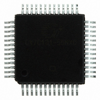
IC SRAM 8KBIT 55NS 52-QFP
Manufacturer
Cypress Semiconductor Corp
Type
Asynchronousr
Specifications of CY7C131-55NXC
Memory Size
8K (1K x 8)
Package / Case
52-QFP
Format - Memory
RAM
Memory Type
SRAM - Dual Port, Asynchronous
Speed
55ns
Interface
Parallel
Voltage - Supply
4.5 V ~ 5.5 V
Operating Temperature
0°C ~ 70°C
Access Time
55 ns
Supply Voltage (max)
5.5 V
Supply Voltage (min)
4.5 V
Maximum Operating Current
110 mA
Maximum Operating Temperature
+ 70 C
Minimum Operating Temperature
0 C
Mounting Style
SMD/SMT
Number Of Ports
2
Operating Supply Voltage
5 V
Rohs Compliant
YES
Lead Free Status / RoHS Status
Lead free / RoHS Compliant
Lead Free Status / RoHS Status
Lead free / RoHS Compliant, Lead free / RoHS Compliant
Other names
428-2111
CY7C131-55NXC
CY7C131-55NXC
Available stocks
Company
Part Number
Manufacturer
Quantity
Price
Company:

Part Number:
CY7C131-55NXC
Manufacturer:
Cypress Semiconductor Corp
Quantity:
10 000
Company:
Part Number:
CY7C131-55NXCT
Manufacturer:
Cypress Semiconductor Corp
Quantity:
10 000


Switching Waveforms
Document Number: 38-06002 Rev. *G
Notes
ADDRESS
36. The internal write time of the memory is defined by the overlap of CS LOW and R/W LOW. Both signals must be low to initiate a write and either signal can
37. If OE is LOW during a R/W controlled write cycle, the write pulse width must be the larger of t
38. These parameters are measured from the input signal changing, until the output pin goes to a high-impedance state.
39. If the CE LOW transition occurs simultaneously with or after the R/W LOW transition, the outputs remain in the high impedance state.
ADDRESS
DATA
DATA
D
DATA
terminate a write by going high. The data input setup and hold timing should be referenced to the rising edge of the signal that terminates the write.
and for data to be placed on the bus for the required t
OUT
R/W
OE
CE
R/W
IN
OUT
CE
IN
Figure 9. Write Cycle No. 2 (R/W Three-States Data I/Os—Either Port)
Figure 8. Write Cycle No. 1 (OE Three-States Data I/Os—Either Port
t
HZOE
t
SA
(continued)
t
SA
SD
.
t
SCE
t
SCE
t
AW
t
AW
t
Either Port
HZWE
t
WC
t
WC
HIGH IMPEDANCE
t
PWE
DATA VALID
t
PWE
t
SD
PWE
HIGH IMPEDANCE
or t
t
DATA VALID
SD
HZWE
+ t
SD
to allow the data I/O pins to enter high impedance
t
HD
t
HD
t
LZWE
t
HA
t
HA
CY7C130, CY7C130A
CY7C131, CY7C131A
[36, 37]
[38, 39]
Page 12 of 22
[+] Feedback
Related parts for CY7C131-55NXC
Image
Part Number
Description
Manufacturer
Datasheet
Request
R

Part Number:
Description:
IC SRAM 8KBIT 25NS 52PLCC
Manufacturer:
Cypress Semiconductor Corp
Datasheet:
Part Number:
Description:
IC SRAM 8KBIT 55NS 52PLCC
Manufacturer:
Cypress Semiconductor Corp
Datasheet:
Part Number:
Description:
IC SRAM 8KBIT 15NS 52PLCC
Manufacturer:
Cypress Semiconductor Corp
Datasheet:
Part Number:
Description:
IC SRAM 8KBIT 25NS 52PLCC
Manufacturer:
Cypress Semiconductor Corp
Datasheet:
Part Number:
Description:
IC SRAM 8KBIT 35NS 52PLCC
Manufacturer:
Cypress Semiconductor Corp
Datasheet:
Part Number:
Description:
IC SRAM 8KBIT 15NS 52PLCC
Manufacturer:
Cypress Semiconductor Corp
Datasheet:
Part Number:
Description:
IC SRAM 8KBIT 15NS 52PLCC
Manufacturer:
Cypress Semiconductor Corp
Datasheet:
Part Number:
Description:
IC SRAM 8KBIT 55NS 52PLCC
Manufacturer:
Cypress Semiconductor Corp
Datasheet:

Part Number:
Description:
IC,SRAM,1KX8,CMOS,LDCC,52PIN,PLASTIC
Manufacturer:
Cypress Semiconductor Corp
Datasheet:
Part Number:
Description:
IC,SRAM,1KX8,CMOS,QFP,52PIN,PLASTIC
Manufacturer:
Cypress Semiconductor Corp
Datasheet:
Part Number:
Description:
Manufacturer:
Cypress Semiconductor Corp
Datasheet:

Part Number:
Description:
Manufacturer:
Cypress Semiconductor Corp
Datasheet:
Part Number:
Description:
SRAM Chip Async Dual 5V 8K-Bit 1K x 8 15ns 52-Pin PLCC
Manufacturer:
Cypress Semiconductor Corp
Datasheet:
Part Number:
Description:
CY7C131-15NXI
Manufacturer:
Cypress Semiconductor Corp
Datasheet:
Part Number:
Description:
CY7C131-25JXCT
Manufacturer:
Cypress Semiconductor Corp
Datasheet: