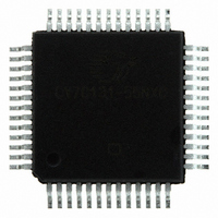
CY7C131-55NXC Cypress Semiconductor Corp, CY7C131-55NXC Datasheet - Page 8

CY7C131-55NXC
Manufacturer Part Number
CY7C131-55NXC
Description
IC SRAM 8KBIT 55NS 52-QFP
Manufacturer
Cypress Semiconductor Corp
Type
Asynchronousr
Specifications of CY7C131-55NXC
Memory Size
8K (1K x 8)
Package / Case
52-QFP
Format - Memory
RAM
Memory Type
SRAM - Dual Port, Asynchronous
Speed
55ns
Interface
Parallel
Voltage - Supply
4.5 V ~ 5.5 V
Operating Temperature
0°C ~ 70°C
Access Time
55 ns
Supply Voltage (max)
5.5 V
Supply Voltage (min)
4.5 V
Maximum Operating Current
110 mA
Maximum Operating Temperature
+ 70 C
Minimum Operating Temperature
0 C
Mounting Style
SMD/SMT
Number Of Ports
2
Operating Supply Voltage
5 V
Rohs Compliant
YES
Lead Free Status / RoHS Status
Lead free / RoHS Compliant
Lead Free Status / RoHS Status
Lead free / RoHS Compliant, Lead free / RoHS Compliant
Other names
428-2111
CY7C131-55NXC
CY7C131-55NXC
Available stocks
Company
Part Number
Manufacturer
Quantity
Price
Company:
Part Number:
CY7C131-55NXC
Manufacturer:
Cypress Semiconductor Corp
Quantity:
10 000
Company:
Part Number:
CY7C131-55NXCT
Manufacturer:
Cypress Semiconductor Corp
Quantity:
10 000
Switching Characteristics
Over the Operating Range
Document Number: 38-06002 Rev. *G
t
t
t
t
t
t
t
t
t
t
t
t
t
t
t
t
Shaded areas contain preliminary information.
Notes
BLA
BHA
BLC
BHC
PS
WB
WH
BDD
DDD
WDD
WINS
EINS
INS
OINR
EINR
INR
20. These parameters are measured from the input signal changing, until the output pin goes to a high-impedance state.
21. CY7C140/CY7C141 only.
22. A write operation on Port A, where Port A has priority, leaves the data on Port B’s outputs undisturbed until one access time after one of the following:
Busy/Interrupt Timing
Interrupt Timing
Parameter
[21]
BUSY on Port B goes HIGH.
Port B’s address is toggled.
CE for Port B is toggled.
R/W for Port B is toggled during valid read.
BUSY LOW from address match
BUSY HIGH from address mismatch
BUSY LOW from CE LOW
BUSY HIGH from CE HIGH
Port set-up for priority
R/W LOW after BUSY LOW
R/W HIGH after BUSY HIGH
BUSY HIGH to valid data
Write data valid to read data valid
Write pulse to data delay
R/W to INTERRUPT set time
CE to INTERRUPT set time
Address to INTERRUPT set time
OE to INTERRUPT reset time
CE to INTERRUPT reset time
Address to INTERRUPT reset time
[12, 13]
(continued)
Description
[20]
[20]
[20]
[20]
[20]
7C131-15
Min
13
7C131A-15
–
–
–
–
5
0
–
–
–
–
–
–
–
–
–
7C141-15
Note 22
Note 22
Max
15
15
15
15
15
15
15
15
15
15
15
[14]
–
–
–
Min
7C130-25
20
–
–
–
–
5
0
–
–
–
–
–
–
–
–
–
7C131-25
7C140-25
7C141-25
Note 22
Note 22
Max
20
20
20
20
25
25
25
25
25
25
25
CY7C130, CY7C130A
CY7C131, CY7C131A
[14]
–
–
–
Min
7C130A-30
30
–
–
–
–
5
0
–
–
–
–
–
–
–
–
–
7C130-30
7C131-30
7C140-30
7C141-30
Note 22
Note 22
Max
20
20
20
20
30
25
25
25
25
25
25
–
–
–
Page 8 of 22
Unit
ns
ns
ns
ns
ns
ns
ns
ns
ns
ns
ns
ns
ns
ns
ns
ns
[+] Feedback


