DS2431X-S+ Maxim Integrated Products, DS2431X-S+ Datasheet
DS2431X-S+
Specifications of DS2431X-S+


Related parts for DS2431X-S+


DS2431X-S+ Summary of contents
Page 1
... PART DS2431+ DS2431+T&R DS2431P+ DS2431P+T&R DS2431G+ DS2431G+T&R DS2431Q+T&R IO DS2431X-S+ DS2431 DS2431X+ Note: The leads of TO-92 packages on tape and reel are formed to approximately 100-mil (2.54mm) spacing. For details, refer to the package outline drawing. GND + Denotes a lead(Pb)-free/RoHS-compliant package. T&R = Tape and reel. ...
Page 2
EEPROM ABSOLUTE MAXIMUM RATINGS IO Voltage Range to GND .......................................-0.5V to +6V IO Sink Current ...................................................................20mA Operating Temperature Range ...........................-40°C to +85°C Junction Temperature ......................................................+150°C Storage Temperature Range .............................-55°C to +125°C Stresses beyond those listed under “Absolute Maximum ...
Page 3
ELECTRICAL CHARACTERISTICS (continued -40°C to +85°C.) (Note 1) A PARAMETER SYMBOL IO PIN: 1-Wire WRITE Write-Zero Low Time (Notes 2, 16, 17) Write-One Low Time (Notes 2, 17) IO PIN: 1-Wire READ Read Low Time (Notes 2, 18) ...
Page 4
EEPROM Note 19: Current drawn from IO during the EEPROM programming interval. The pullup circuit on IO during the programming interval should be such that the voltage greater than or equal to V impedance bypass ...
Page 5
... The DS2431 has an additional memory area called the scratchpad that acts as a buffer when writing to the main memory or the register page. Data is first written to the scratchpad from which it can be read back. After the data has been verified, a Copy Scratchpad command transfers the data to its final memory location ...
Page 6
... The protocol for these memory function commands is described in Figure 7. All data is read and written least significant bit first. iButton is a registered trademark of Maxim Integrated Products, Inc. 6 _______________________________________________________________________________________ AVAILABLE COMMANDS: DATA FIELD AFFECTED: READ ROM 64-BIT REG ...
Page 7
... Figure 4. 1-Wire CRC Generator Memory Access Data memory and registers are located in a linear address space, as shown in Figure 5. The data memory and the registers have unrestricted read access. The DS2431 EEPROM array consists of 18 rows of 8 bytes each. The first 16 rows are divided equally into four memory pages (32 bytes each) ...
Page 8
... Write Scratchpad command is loaded into the scratchpad. A protection setting of 55h (write protect) causes the incoming data to be ignored and the target address main memory data to be loaded into the scratchpad. A protection setting of AAh (EPROM mode) causes the logical AND of incoming data and target address main memory data to be loaded into the scratchpad ...
Page 9
... The Memory Function Flowchart (Figure 7) describes the protocols necessary for accessing the memory of the DS2431. An example on how to use these functions to write to and read from the device is in the Memory Function Example section. The communication between the master and the DS2431 takes place either at standard speed (default overdrive speed ( ...
Page 10
... AND DATA BYTES AS THEY WERE SENT BY THE BUS MASTER N BUS MASTER MASTER Tx RESET? Rx "1" ROM FUNCTIONS FLOWCHART (FIGURE 9) Figure 7a. Memory Function Flowchart 10 ______________________________________________________________________________________ FROM ROM FUNCTIONS FLOWCHART (FIGURE 9) N READ SCRATCHPAD? BUS MASTER Rx TA1 (T[7:0]), TA2 (T[15:8]), AND E/S BYTE DS2431 SETS ...
Page 11
... BUS MASTER Tx TA1 (T[7:0]), TA2 (T[15:8]) AND E/S BYTE Y AUTH. CODE T[15:0] < 0090h? MATCH? N DURATION: t BUS MASTER Rx "1"s N MASTER Tx RESET FIGURE 7a Figure 7b. Memory Function Flowchart (continued) ______________________________________________________________________________________ 1024-Bit, 1-Wire EEPROM F0h N READ MEMORY? Y BUS MASTER Tx TA1 (T[7:0]), TA2 (T[15:8]) Y ADDRESS < 90h ...
Page 12
... TA2, E/S, in that order). If the pattern matches, the target address is valid, the PF flag is not set, and the target memory is not copy protected, then the AA flag is set and the copy begins. All 8 bytes of scratchpad contents are copied to the target memo- ry location. The duration of the device’ ...
Page 13
... Application Note 187: 1-Wire Search Algorithm for a detailed discussion, including an example. This command can save time in a single-drop bus sys- tem by allowing the bus master to access the memory functions without providing the 64-bit ROM code. If more than one slave is present on the bus and, for ...
Page 14
... BIT 0 MATCH? BIT 0 MATCH DS2431 Tx BIT 1 MASTER Tx BIT 1 DS2431 Tx BIT 1 MASTER Tx BIT BIT 1 MATCH? BIT 1 MATCH DS2431 Tx BIT 63 MASTER Tx BIT 63 DS2431 Tx BIT 63 MASTER Tx BIT BIT 63 MATCH? BIT 63 MATCH MEMORY FUNCTIONS FLOWCHART (FIGURE 7) FROM FIGURE 9b CCh N SKIP ROM COMMAND? TO FIGURE FIGURE 9b FROM FIGURE 9b ...
Page 15
TO FIGURE 9a FROM FIGURE 9a COMMAND? FROM FIGURE 9a TO FIGURE 9a Figure 9b. ROM Functions Flowchart (continued) ______________________________________________________________________________________ 1024-Bit, 1-Wire EEPROM A5h 3Ch N N RESUME OVERDRIVE- OVERDRIVE- SKIP ROM? MATCH ROM ...
Page 16
... DS2431. A reset pulse followed by a presence pulse indicates that the DS2431 is ready to receive data, given the correct ROM and memory function command. If the bus master uses slew-rate control on the falling edge, it must pull down the line for t t duration of 480µ ...
Page 17
MASTER Tx "RESET PULSE" V PUP V IHMASTER ILMAX RESISTOR Figure 10. Initialization Procedure: Reset and Presence Pulse Read/Write Time Slots Data communication with the DS2431 takes place in time slots that ...
Page 18
EEPROM WRITE-ONE TIME SLOT t W1L V PUP V IHMASTER ILMAX RESISTOR WRITE-ZERO TIME SLOT V PUP V IHMASTER ILMAX RESISTOR READ-DATA ...
Page 19
Improved Network Behavior (Switchpoint Hysteresis 1-Wire environment, line termination is possible only during transients controlled by the bus master (1-Wire driver). 1-Wire networks, therefore, are suscep- tible to noise of various origins. Depending on the physical size and ...
Page 20
... Target address TA1, TA2 with E/S byte. <8–T[2:0] bytes> Transfer of as many bytes as needed to reach the end of the scratchpad for a given target address. <Data to EOM> Transfer of as many data bytes as are needed to reach the end of the memory. CRC-16 Transfer of an inverted CRC-16. FF Loop Indefinite loop where the master reads FF bytes ...
Page 21
... RST PD Select CPS TA-E/S Programming AA Loop Copy Scratchpad (Invalid Address Copy Protected) RST PD Select CPS TA-E/S FF Loop Read Memory (Success) RST PD Select RM TA <Data to EOM> FF Loop Read Memory (Invalid Address) RST PD Select Loop ______________________________________________________________________________________ 1024-Bit, 1-Wire EEPROM Programming 1-Wire Communication Examples ...
Page 22
... EEPROM Memory Function Example Write to the first 8 bytes of memory page 1. Read the entire memory. MASTER MODE — ______________________________________________________________________________________ With only a single DS2431 connected to the bus mas- ter, the communication looks like this: DATA (LSB FIRST) (Reset) Reset pulse (Presence) ...
Page 23
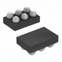
SIDE VIEW FRONT VIEW GND N. FRONT VIEW (T&R VERSION) TO- TOP VIEW + GND N.C. DS2431 4 N.C. 3 N.C. TSOC TOP VIEW ...
Page 24
EEPROM For the latest package outline information and land patterns www.maxim-ic.com/packages. Note that a “+”, “#”, or “-” in the package code indicates RoHS status only. Package drawings may show a different suffix character, but the ...
Page 25
... A2 (see also pages 1, 13). Removed t FPD 0.8mA to match GBD. Updated Memory Function Example table. Added CSP package outline drawing number to Pin Configuration. Changed V TL(MIN) In the Absolute Maximum Ratings, changed storage temp to -55°C to +125°C; in the ...
Page 26
... Maxim cannot assume responsibility for use of any circuitry other than circuitry entirely embodied in a Maxim product. No circuit patent licenses are implied. Maxim reserves the right to change the circuitry and specifications without notice at any time. 26 ____________________Maxim Integrated Products, 120 San Gabriel Drive, Sunnyvale, CA 94086 408-737-7600 © 2011 Maxim Integrated Products ...