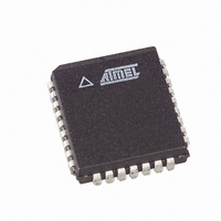
AT49LH004-33JC SL383 Atmel, AT49LH004-33JC SL383 Datasheet - Page 25

AT49LH004-33JC SL383
Manufacturer Part Number
AT49LH004-33JC SL383
Description
IC FLASH 4MBIT 33MHZ 32PLCC
Manufacturer
Atmel
Datasheet
1.AT49LH004-33JC.pdf
(40 pages)
Specifications of AT49LH004-33JC SL383
Format - Memory
FLASH
Memory Type
FLASH
Memory Size
4M (512K x 8)
Speed
33MHz
Interface
Parallel
Voltage - Supply
3 V ~ 3.6 V
Operating Temperature
0°C ~ 85°C
Package / Case
32-PLCC
Lead Free Status / RoHS Status
Contains lead / RoHS non-compliant
14.1
14.2
14.3
14.4
15. Device Operation
3383D–FLASH–6/05
Bus Operation
Output Disable/Enable
Row/Column Addresses
RDY/BSY
Four control pins dictate the flow of data into and out of the device: R/C, OE, WE, and RST.
The R/C pin is the A/A Mux interface control pin used to latch row and column addresses. OE
is the data output control pin for the I/O[7:0] lines and, when active, drives the selected mem-
ory data onto the I/O bus (WE and RST must be at VIH). The WE pin controls the flow of data
into the device. Addresses previously captured by the R/C pin transitions and data are latched
into the device on the rising edge of WE. The RST pin is used to reset the device.
All A/A Mux bus cycles can be conformed to operate on most automated test equipment and
PROM programmers.
Table 14-1.
Notes:
With OE at a logic-high level (V
placed in the high-impedance state. With OE at a logic-low level (V
enabled. Output pins I/O[7:0] are placed in an output-drive state.
R/C is the A/A Mux interface control pin used to latch row (A10 - A0) and column address
(A18 - A11) values presented on the A[10:0] pins. R/C latches row addresses on the falling
edge and column addresses on the rising edge.
The open-drain Ready/Busy output pin provides a hardware method of detecting the end of a
program or erase operation. RDY/BSY is actively pulled low during the internal program and
erase cycles and is released at the completion of the cycle.
The FWH/LPC and A/A Mux interfaces should be considered hardware interfaces that can be
used to transfer commands and data to and from the device. The device commands detailed
in
Since the FWH/LPC interface communicates using a 4-bit data bus and the A/A Mux interface
utilizes an 8-bit data bus, the number of interface bus cycles needed to perform an operation
will vary. For example, when using the FWH/LPC interface, 17 PCI clock cycles are required
for a FWH or LPC memory write cycle. Therefore, for one “write” device command cycle,
17 FWH/LPC bus cycles are needed. Likewise, for one “read” device command cycle using
the FWH/LPC interface, 19 FWH/LPC bus cycles are required.
Mode
Read
Output Disable
Write
Product ID Read
“Command Definitions Table” on page 26
(1)(2)
(1)(2)
1. X can be V
2. V
3. Refer to
V
IH
IL
min = 0.5V, V
and V
(1)(2)
A/A Mux Interface Bus Operations
(1)(2)(3)
Table 16-2
IL
IL
refer to the DC characteristics associated with the Flash memory output buffers:
or V
IH
IL
max = 0.8V, V
for control and address input pins.
for Product ID addresses and data.
RST
V
V
V
V
IH
IH
IH
IH
IH
), the device outputs are disabled. Output pins I/O[7:0] are
IH
min = 2.0V, V
can be issued using either interface.
OE
V
V
V
V
IH
IH
IL
IL
IH
max = V
WE
V
V
V
V
IH
IH
IH
IL
CC
+ 0.5V.
IL
), the device outputs are
Address
Note 3
AT49LH004
X
X
X
I/O[7:0]
High-Z
Note 3
D
D
OUT
IN
25


