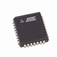
AT49LH004-33JC SL383 Atmel, AT49LH004-33JC SL383 Datasheet - Page 5

AT49LH004-33JC SL383
Manufacturer Part Number
AT49LH004-33JC SL383
Description
IC FLASH 4MBIT 33MHZ 32PLCC
Manufacturer
Atmel
Datasheet
1.AT49LH004-33JC.pdf
(40 pages)
Specifications of AT49LH004-33JC SL383
Format - Memory
FLASH
Memory Type
FLASH
Memory Size
4M (512K x 8)
Speed
33MHz
Interface
Parallel
Voltage - Supply
3 V ~ 3.6 V
Operating Temperature
0°C ~ 85°C
Package / Case
32-PLCC
Lead Free Status / RoHS Status
Contains lead / RoHS non-compliant
Table 5-1.
3383D–FLASH–6/05
Symbol
WP
ID[3:0]
GPI[4:0]
A[10:0]
I/O[7:0]
R/C
OE
WE
Name and Function
WRITE PROTECT: The WP pin is used to protect all remaining sectors that are not
being used for the top boot region.
details.
If the WP pin is high, then hardware write protection for all of the sectors except the
top boot sector will be disabled. Register-based sector protection, however, will still
apply. The state of the WP pin does not affect the state of the Sector Locking
Registers.
This pin is used as the A5 pin in the A/A Mux interface.
IDENTIFICATION INPUTS: These four pins are part of the mechanism that allows
multiple devices to be attached to the same bus. The strapping of these pins is
used to assign an ID to each device. The boot device must have ID[3:0] = 0000,
and it is recommended that all subsequent devices should use sequential up-count
strapping (e.g., 0001, 0010, 0011, etc.).
The ID[3:0] pins are internally pulled-down with resistors valued between 20 kΩ
and 100 kΩ when using the FWH/LPC interface, so connection of these pins is not
necessary if only a single device will be used in a system. Any pins intended to be
low may be left floating. Any ID pin driven high will exhibit some leakage current.
These pins are used as the A[3:0] pins in the A/A Mux interface.
GENERAL-PURPOSE INPUTS: The individual GPI pins can be used for additional
board flexibility. The state of the GPI pins can be read, using the FWH/LPC
interface, through the GPI register. The GPI pins should be at their desired state
before the start of the PCI clock cycle during which the read is attempted, and they
should remain at the same level until the end of the read cycle.
The voltages applied to the GPI pins must comply with the devices V
requirements. Any unused GPI pins must not be left floating.
These pins are used as the A[10:6] pins in the A/A Mux interface.
ADDRESS INPUTS: These pins are used for inputting the multiplexed address
values when using the A/A Mux interface. The addresses are latched by the rising
and falling edge of R/C pin.
DATA INPUTS/OUTPUTS: The I/O pins are used in the A/A Mux interface to input
data and commands during write cycles and to output data during memory array,
Status Register, and identifier code read cycles. Data is internally latched during a
write cycle.
The I/O pins will be in a high-impedance state when the outputs are disabled.
ROW/COLUMN ADDRESS SELECT: In the A/A Mux interface, the R/C pin is used
to latch the address values presented on the A[10:0] pins. The row addresses
(A10 - 0) are latched on the falling edge of R/C, and the column addresses
(A18 - A11) are latched on the rising edge of R/C.
OUTPUT ENABLE: The OE pin is used in the A/A Mux interface to control the
device’s output buffers during a read cycle.
The I/O[7:0] pins will be in high-impedance state when the OE pin is deasserted
(high).
WRITE ENABLE: The WE pin is used in the A/A Mux interface to control write
operations to the device.
Signal Descriptions (Continued)
See “Sector Protection” on page 17.
IH
and V
for more
IL
FWH/LPC
X
X
X
Interface
AT49LH004
A/A Mux
X
X
X
X
X
Output
Input/
Type
Input
Input
Input
Input
Input
Input
Input
5


