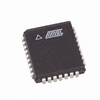
AT49LH004-33JC SL383 Atmel, AT49LH004-33JC SL383 Datasheet - Page 8

AT49LH004-33JC SL383
Manufacturer Part Number
AT49LH004-33JC SL383
Description
IC FLASH 4MBIT 33MHZ 32PLCC
Manufacturer
Atmel
Datasheet
1.AT49LH004-33JC.pdf
(40 pages)
Specifications of AT49LH004-33JC SL383
Format - Memory
FLASH
Memory Type
FLASH
Memory Size
4M (512K x 8)
Speed
33MHz
Interface
Parallel
Voltage - Supply
3 V ~ 3.6 V
Operating Temperature
0°C ~ 85°C
Package / Case
32-PLCC
Lead Free Status / RoHS Status
Contains lead / RoHS non-compliant
7.3
7.3.1
7.3.2
7.3.3
7.3.4
8
FWH Memory Cycles
AT49LH004
Start Field
IDSEL (Device Select) Field
MADDR (Memory Address) Field
MSIZE (Memory Size) Field
A valid FWH memory cycle begins with the host driving the FWH4/LFRAME signal low for one
or more clock cycles. While the FWH4/LFRAME signal is low, a valid START value of either
1101b (FWH memory read) or 1110b (FWH memory write) must be driven on the
FWH/LAD[3:0] pins. Following the START field, an IDSEL (Device Select) field must be sent to
the device. The IDSEL field acts like a chip select in that it indicates which device should
respond to the current operation. After the IDSEL field has been sent, the 7-clock MADDR
(Memory Address) field must be sent to the device to provide the 28-bit starting address loca-
tion of where to begin reading or writing in the memory. Following the MADDR field, the
MSIZE (Memory Size) field must be sent to indicate the number of bytes to transfer.
Figure 7-1.
This 1-clock field indicates the start of a cycle. It is valid on the last clock that FWH4/LFRAME
is sampled low. The two start fields that are used for a FWH cycle are: 1101b to indicate a
FWH memory read cycle and 1110b to indicate a FWH memory write cycle. If the start field
that is sampled is not one of these values, then the cycle attempted is not a FWH memory
cycle. It may be a valid LPC memory cycle that the device will attempt to decode.
This 1-clock field is used to indicate which FWH component in the system is being selected.
The four bits transmitted over FWH/LAD[3:0] during this clock are compared with values
strapped on the ID[3:0] pins. If there is a match, the device will continue to decode the cycle to
determine which bytes are requested on a read or which bytes to update on a write. If there
isn’t a match, the device may discard the rest of the cycle and go into a standby power state.
This is a 7-clock field that is used to provide a 28-bit (A27 - A0) memory address. This allows
for provisioning of up to 256 MB per FWH memory device, for a total of a 4 GB addressable
space if 16 FWH memory devices (256 MB each) were used in a system.
The AT49LH004 only decodes the last six MADDR nibbles (A23 - A0) and ignores address
bits A27 - A23 and A21 - A19. Address bit A22 is used to determine whether reads or writes to
the device will be directed to the memory array (A22 = 1) or to the register space (A22 = 0).
Addresses are transferred to the device with the most significant nibble first.
The 1-clock MSIZE is used to indicate how many bytes of data will be transferred during a
read or write. The AT49LH004 only supports single-byte transfers, so 0000b must be sent in
this field to indicate a single-byte transfer.
FWH4/LFRAME
FWH/LAD[3:0]
CLK
FWH Memory Cycle Initiation and Addressing
START
IDSEL
MADDR MADDR MADDR
MADDR
MADDR MADDR MADDR
3383D–FLASH–6/05
MSIZE


