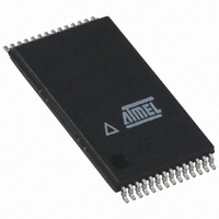
AT45DB642D-TU Atmel, AT45DB642D-TU Datasheet - Page 17

AT45DB642D-TU
Manufacturer Part Number
AT45DB642D-TU
Description
IC FLASH 64MBIT 66MHZ 28TSOP
Manufacturer
Atmel
Datasheet
1.AT45DB642D-CU.pdf
(58 pages)
Specifications of AT45DB642D-TU
Format - Memory
FLASH
Memory Type
DataFLASH
Memory Size
64M (8192 pages x 1056 bytes)
Speed
66MHz
Interface
Parallel/Serial
Voltage - Supply
2.7 V ~ 3.6 V
Operating Temperature
-40°C ~ 85°C
Package / Case
28-TSOP
Density
64Mb
Access Time (max)
6ns
Interface Type
Parallel/Serial-SPI
Boot Type
Not Required
Address Bus
1/8Bit
Operating Supply Voltage (typ)
3.3V
Operating Temp Range
-40C to 85C
Package Type
TSOP-I
Program/erase Volt (typ)
2.7 to 3.6V
Sync/async
Synchronous
Operating Temperature Classification
Industrial
Operating Supply Voltage (min)
2.7V
Operating Supply Voltage (max)
3.6V
Word Size
8b
Number Of Words
8M
Supply Current
15mA
Mounting
Surface Mount
Pin Count
28
Data Bus Width
8 bit
Architecture
Sectored
Supply Voltage (max)
3.6 V
Supply Voltage (min)
2.7 V
Maximum Operating Current
15 mA
Mounting Style
SMD/SMT
Organization
256 KB x 32
Memory Configuration
8192 Pages X 1056 Bytes
Clock Frequency
66MHz
Supply Voltage Range
2.7V To 3.6V
Memory Case Style
TSOP
Rohs Compliant
Yes
Lead Free Status / RoHS Status
Lead free / RoHS Compliant
Available stocks
Company
Part Number
Manufacturer
Quantity
Price
Company:
Part Number:
AT45DB642D-TU
Manufacturer:
MICRON
Quantity:
101
Company:
Part Number:
AT45DB642D-TU
Manufacturer:
ATMEL
Quantity:
9 396
Company:
Part Number:
AT45DB642D-TU
Manufacturer:
AT
Quantity:
5
Part Number:
AT45DB642D-TU
Manufacturer:
ATMEL/爱特梅尔
Quantity:
20 000
Figure 9-3.
9.1.3
Figure 9-4.
3542K–DFLASH–04/09
SI or IO
SO or IO
SI or IO
7
Read Sector Protection Register Command
- IO
7
7
CS
- IO
- IO
Program Sector Protection Register
Read Sector Protection Register
CS
0
0
0
Each transition
represents 8 bits
Each transition
represents 8 bits
The Program Sector Protection Register command utilizes the internal SRAM buffer for process-
ing. Therefore, the contents of the buffer will be altered from its previous state when this
command is issued.
To read the Sector Protection Register, the CS pin must first be asserted. Once the CS pin has
been asserted, an opcode of 32H and a series of dummy bytes (3 dummy bytes if using the
serial interface or 7 dummy bytes if using the 8-bit interface) must be clocked in via the SI or I/O7
or I/O0 pins. After the last bit of the opcode and dummy bytes have been clocked in, any addi-
tional clock pulses on the SCK/CLK pins will result in data for the content of the Sector
Protection Register being output on the SO or I/O7-I/O0 pins. The first byte corresponds to sec-
tor 0 (0a, 0b), the second byte corresponds to sector 1 and the last byte (byte 32) corresponds to
sector 31. Once the last byte of the Sector Protection Register has been clocked out, any addi-
tional clock pulses will result in undefined data being output on the SO or I/O pins. The CS must
be deasserted to terminate the Read Sector Protection Register operation and put the output
into a high-impedance state.
Note:
Command
Program Sector Protection Register
Command
Read Sector Protection Register
Opcode
Byte 1
Opcode
xx = Dummy Byte
Opcode
Byte 2
X
Opcode
Byte 3
Serial Interface = 3 Dummy Bytes
X
Opcode
Byte 4
X
Byte 1
Byte 1
3DH
32H
Data Byte
Data Byte
n
n
Data Byte
Byte 2
Byte 2
2AH
xxH
n + 1
Data Byte
n + 1
8-bit Interface = 7 Dummy Bytes
Byte 3
Byte 3
7FH
xxH
Data Byte
n + 31
Data Byte
n + 31
Byte 4
Byte 4
FCH
xxH
17


