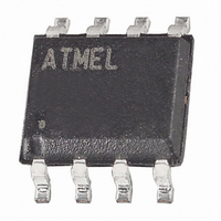
AT45DB021D-SH-B Atmel, AT45DB021D-SH-B Datasheet - Page 7

AT45DB021D-SH-B
Manufacturer Part Number
AT45DB021D-SH-B
Description
IC FLASH 2MBIT 66MHZ 8SOIC
Manufacturer
Atmel
Specifications of AT45DB021D-SH-B
Format - Memory
FLASH
Memory Type
DataFLASH
Memory Size
2M (1024 pages x 264 bytes)
Speed
66MHz
Interface
SPI, RapidS
Voltage - Supply
2.7 V ~ 3.6 V
Operating Temperature
-40°C ~ 85°C
Package / Case
8-SOIC (5.3mm Width), 8-SOP, 8-SOEIAJ
Architecture
Sectored
Interface Type
SPI Serial
Supply Voltage (max)
3.6 V
Supply Voltage (min)
2.7 V
Maximum Operating Current
15 mA
Mounting Style
SMD/SMT
Organization
32 KB x 8
Memory Configuration
1024 Pages X 264 Bytes
Clock Frequency
66MHz
Supply Voltage Range
2.7V To 3.6V
Memory Case Style
SOIC
Rohs Compliant
Yes
Lead Free Status / RoHS Status
Lead free / RoHS Compliant
Other names
AT45DB021D-SU
AT45DB021D-SU
AT45DB021D-SU
Available stocks
Company
Part Number
Manufacturer
Quantity
Price
Part Number:
AT45DB021D-SH-B
Manufacturer:
ATMEL/爱特梅尔
Quantity:
20 000
3638J–DFLASH–5/10
5.
5.1
5.2
5.3
read data from the buffer. The D4H opcode can be used at any SCK frequency up to the maximum specified by
f
To perform a buffer read from the Atmel
the device followed by three address bytes comprised of 15 don’t care bits and 9 buffer address bits (BFA8 -
followed by three address bytes comprised of 16 don’t care bits and eight buffer address bits (BFA7 - BFA0).
Following the address bytes, one don’t care byte must be clocked in to initialize the read operation. The CS pin
must remain low during the loading of the opcode, the address bytes, the don’t care bytes, and the reading of data.
When the end of a buffer is reached, the device will continue reading back at the beginning of the buffer. A low-to-
high transition on the CS pin will terminate the read operation and tri-state the output pin (SO).
Program and Erase Commands
Buffer Write
Data can be clocked in from the input pin (SI) into the buffer. To load data into the DataFlash standard buffer (264-
bytes), a 1-byte opcode, 84H, must be clocked into the device followed by three address bytes comprised of 15
don’t care bits and nine buffer address bits (BFA8 - BFA0). The nine buffer address bits specify the first byte in the
buffer to be written. To load data into the binary buffers (256-bytes each), a 1-byte opcode, 84H, must be clocked
into the device followed by three address bytes comprised of 16 don’t care bits and eight buffer address bits (BFA7
- BFA0). The eight buffer address bits specify the first byte in the buffer to be written. After the last address byte
has been clocked into the device, data can then be clocked in on subsequent clock cycles. If the end of the data
buffer is reached, the device will wrap around back to the beginning of the buffer. Data will continue to be loaded
into the buffer until a low-to-high transition is detected on the CS pin.
Buffer to Main Memory Page Program with Built-in Erase
Data written into the buffer can be programmed into the main memory. A 1-byte opcode, 83H, must be clocked into
the device. For the DataFlash standard page size (264-bytes), the opcode must be followed by three address bytes
consist of five don’t care bits, 10 page address bits (PA9 - PA0) that specify the page in the main memory to be
written and nine don’t care bits. To perform a buffer to main memory page program with built-in erase for the binary
page size (256-bytes), the opcode 83H must be clocked into the device followed by three address bytes consisting
of six don’t care bits, 10 page address bits (A17 - A8) that specify the page in the main memory to be written and
eight don’t care bits. When a low-to-high transition occurs on the CS pin, the part will first erase the selected page
in main memory (the erased state is a logic 1) and then program the data stored in the buffer into the specified
page in main memory. Both the erase and the programming of the page are internally self-timed and should take
place in a maximum time of t
Buffer to Main Memory Page Program without Built-in Erase
A previously-erased page within main memory can be programmed with the contents of the buffer. A 1-byte
opcode, 88H, must be clocked into the device. For the DataFlash standard page size (264-bytes), the opcode must
be followed by three address bytes consist of five don’t care bits, 10 page address bits (PA9 - PA0) that specify the
page in the main memory to be written and nine don’t care bits. To perform a buffer to main memory page program
without built-in erase for the binary page size (256-bytes), the opcode 88H must be clocked into the device
followed by three address bytes consisting of six don’t care bits, 10 page address bits (A17 - A8) that specify the
page in the main memory to be written and eight don’t care bits. When a low-to-high transition occurs on the CS
pin, the part will program the data stored in the buffer into the specified page in the main memory. It is necessary
that the page in main memory that is being programmed has been previously erased using one of the erase
commands (Page Erase or Block Erase). The programming of the page is internally self-timed and should take
place in a maximum time of t
CAR1
BFA0). To perform a buffer read from the binary buffer (256-bytes), the opcode must be clocked into the device
. The D1H opcode can be used for lower frequency read operations up to the maximum specified by f
EP
P
. During this time, the status register will indicate that the part is busy.
. During this time, the status register will indicate that the part is busy.
®
DataFlash
®
standard buffer (264-bytes), the opcode must be clocked into
Atmel AT45DB021D
CAR2
.
7


