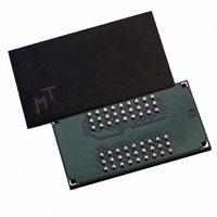
MT48H8M16LFB4-8 IT:J TR Micron Technology Inc, MT48H8M16LFB4-8 IT:J TR Datasheet - Page 38

MT48H8M16LFB4-8 IT:J TR
Manufacturer Part Number
MT48H8M16LFB4-8 IT:J TR
Description
IC SDRAM 128MBIT 125MHZ 54VFBGA
Manufacturer
Micron Technology Inc
Type
Mobile SDRAMr
Datasheet
1.MT48H8M16LFB4-8_ITJ_TR.pdf
(75 pages)
Specifications of MT48H8M16LFB4-8 IT:J TR
Format - Memory
RAM
Memory Type
Mobile SDRAM
Memory Size
128M (8Mx16)
Speed
125MHz
Interface
Parallel
Voltage - Supply
1.7 V ~ 1.9 V
Operating Temperature
-40°C ~ 85°C
Package / Case
54-VFBGA
Organization
8Mx16
Density
128Mb
Address Bus
14b
Access Time (max)
8/6ns
Maximum Clock Rate
125MHz
Operating Supply Voltage (typ)
1.8V
Package Type
VFBGA
Operating Temp Range
-40C to 85C
Operating Supply Voltage (max)
1.95V
Operating Supply Voltage (min)
1.7V
Supply Current
50mA
Pin Count
54
Mounting
Surface Mount
Operating Temperature Classification
Industrial
Lead Free Status / RoHS Status
Lead free / RoHS Compliant
Other names
557-1236-2
Burst Type
Table 19:
CAS Latency (CL)
PDF: 09005aef832ff1ea/Source: 09005aef832ff1ac
sdr_mobile_sdram_cmd_op_timing_dia_fr10_08__3.fm - Rev. E 4/09 EN
Burst Length
Continuous
2
4
8
Burst Definition Table
n = A0–An/9/8 (location 0–y)
Starting Column Address
A2
0
0
0
0
1
1
1
1
Accesses within a given burst can be programmed to be either sequential or interleaved;
this is referred to as the burst type and is selected via bit M3.
The ordering of accesses within a burst is determined by the BL, the burst type, and the
starting column address, as shown in Table 19.
The CL is the delay, in clock cycles, between the registration of a READ command and
the availability of the output data. The latency can be set to two or three clocks.
If a READ command is registered at clock edge n, and the latency is m clocks, the data
will be available by clock edge n + m. The DQ start driving as a result of the clock edge
one cycle earlier (n + m - 1), and provided that the relevant access times are met, the data
is valid by clock edge n + m. For example, assuming that the clock cycle time is such that
all relevant access times are met, if a READ command is registered at T0 and the latency
is programmed to two clocks, the DQ start driving after T1 and the data is valid by T2, as
shown in Figure 15 on page 39.
Reserved states should not be used as unknown operation or incompatibility with future
versions may result.
A1
A1
0
0
1
1
0
0
1
1
0
0
1
1
A0
A0
A0
0
1
0
1
0
1
0
1
0
1
0
1
0
1
128Mb: 8 Meg x 16, 4 Meg x 32 Mobile SDRAM
Type = Sequential
Cn + 3...Cn - 1, Cn...
38
Cn, Cn + 1, Cn + 2,
0-1-2-3-4-5-6-7
1-2-3-4-5-6-7-0
2-3-4-5-6-7-0-1
3-4-5-6-7-0-1-2
4-5-6-7-0-1-2-3
5-6-7-0-1-2-3-4
6-7-0-1-2-3-4-5
7-0-1-2-3-4-5-6
0-1-2-3
1-2-3-0
2-3-0-1
3-0-1-2
0-1
1-0
Order of Accesses Within a Burst
Micron Technology, Inc., reserves the right to change products or specifications without notice.
Type = Interleaved
©2008 Micron Technology, Inc. All rights reserved.
Register Definition
0-1-2-3-4-5-6-7
1-0-3-2-5-4-7-6
2-3-0-1-6-7-4-5
3-2-1-0-7-6-5-4
4-5-6-7-0-1-2-3
5-4-7-6-1-0-3-2
6-7-4-5-2-3-0-1
7-6-5-4-3-2-1-0
Not supported
0-1-2-3
1-0-3-2
2-3-0-1
3-2-1-0
0-1
1-0


