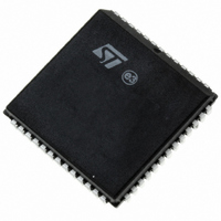
PSD813F1A-90JI STMicroelectronics, PSD813F1A-90JI Datasheet - Page 21

PSD813F1A-90JI
Manufacturer Part Number
PSD813F1A-90JI
Description
IC FLASH 1MBIT 90NS 52PLCC
Manufacturer
STMicroelectronics
Datasheet
1.PSD813F1A-90U.pdf
(111 pages)
Specifications of PSD813F1A-90JI
Format - Memory
FLASH
Memory Type
FLASH
Memory Size
1M (128K x 8)
Speed
90ns
Interface
Parallel
Voltage - Supply
4.5 V ~ 5.5 V
Operating Temperature
-40°C ~ 85°C
Package / Case
52-PLCC
Lead Free Status / RoHS Status
Contains lead / RoHS non-compliant
Other names
497-1976-5
Available stocks
Company
Part Number
Manufacturer
Quantity
Price
Company:
Part Number:
PSD813F1A-90JI
Manufacturer:
WSI
Quantity:
10
Company:
Part Number:
PSD813F1A-90JI
Manufacturer:
STMicroelectronics
Quantity:
10 000
INSTRUCTIONS
An instruction is defined as a sequence of specific
operations. Each received byte is sequentially de-
coded by the PSD and not executed as a standard
write operation. The instruction is executed when
the correct number of bytes are properly received
and the time between two consecutive bytes is
shorter than the time-out value. Some instructions
are structured to include READ operations after
the initial WRITE operations.
The sequencing of any instruction must be fol-
lowed exactly. Any invalid combination of instruc-
tion bytes or time-out between two consecutive
bytes while addressing Flash memory will reset
the device logic into READ mode (Flash memory
reads like a ROM device). An invalid combination
or time-out while addressing the EEPROM block
will cause the offending byte to be interpreted as a
single operation.
The PSD supports these instructions (see
8., page
Flash memory:
■
■
■
■
■
■
EEPROM:
■
■
■
■
■
■
Erase memory by chip or sector
Suspend or resume sector erase
Program a Byte
Reset to READ mode
Read Flash Identifier value
Read Sector Protection Status
power down mode.
Write data to OTP Row
Read data from OTP Row
Power down memory
Enable Software Data Protect (SDP)
Disable SDP
Return from read OTP Row read mode or
20):
Table
These
8., page
tions, the first two bytes of an instruction are the
coded cycles and are followed by a command byte
or confirmation byte. The coded cycles consist of
writing the data AAh to address X555h during the
first cycle and data 55h to address XAAAh during
the second cycle. Address lines A15-A12 are don’t
cares during the instruction WRITE cycles. How-
ever, the appropriate sector select signal (FSi or
EESi) must be selected.
Power-down Instruction and Power-up Mode
EEPROM Power Down Instruction. The
PROM can enter power down mode with the help
of the EEPROM power down instruction (see
ble 8., page
instruction is decoded, the EEPROM memory can-
not be accessed unless a Return instruction (also
in
power down mode will automatically occur when
the APD circuit is triggered (see section entitled
Automatic Power-down (APD) Unit and Power-
down Mode, page
is not required if the APD circuit is used.
Power-up Mode. The PSD internal logic is reset
upon power-up to the READ mode. Any write op-
eration to the EEPROM is inhibited during the first
5ms following power-up. The FSi and EESi select
signals, along with the write strobe signal, must be
in the false state during power-up for maximum se-
curity of the data contents and to remove the pos-
sibility of a byte being written on the first edge of a
write strobe signal. Any write cycle initiation is
locked when V
Table 8., page
20. For efficient decoding of the instruc-
instructions
20). Once the EEPROM power down
CC
20) is decoded. Alternately, this
is below V
65). Therefore, this instruction
are
LKO
detailed
.
PSD813F1A
in
21/111
Table
EE-
Ta-


