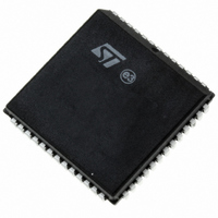
PSD813F1A-90JI STMicroelectronics, PSD813F1A-90JI Datasheet - Page 24

PSD813F1A-90JI
Manufacturer Part Number
PSD813F1A-90JI
Description
IC FLASH 1MBIT 90NS 52PLCC
Manufacturer
STMicroelectronics
Datasheet
1.PSD813F1A-90U.pdf
(111 pages)
Specifications of PSD813F1A-90JI
Format - Memory
FLASH
Memory Type
FLASH
Memory Size
1M (128K x 8)
Speed
90ns
Interface
Parallel
Voltage - Supply
4.5 V ~ 5.5 V
Operating Temperature
-40°C ~ 85°C
Package / Case
52-PLCC
Lead Free Status / RoHS Status
Contains lead / RoHS non-compliant
Other names
497-1976-5
Available stocks
Company
Part Number
Manufacturer
Quantity
Price
Company:
Part Number:
PSD813F1A-90JI
Manufacturer:
WSI
Quantity:
10
Company:
Part Number:
PSD813F1A-90JI
Manufacturer:
STMicroelectronics
Quantity:
10 000
PSD813F1A
Writing to the EEPROM
Data may be written a byte at a time to the EE-
PROM using simple write operations, much like
writing to an SRAM. Unlike SRAM though, the
completion of each byte write must be checked be-
fore the next byte is written. To speed up this pro-
cess, the PSD offers a Page write feature to allow
writing of several bytes before checking status.
To prevent inadvertent writes to EEPROM, the
PSD offers a Software Data Protect (SDP) mode.
Once enabled, SDP forces the MCU to “unlock”
the EEPROM before altering its contents, much
like Flash memory programming.
Writing a Byte to EEPROM. A write operation is
initiated when an EEPROM select signal (EESi) is
true and the write strobe signal (WR) into the PSD
is true. If the PSD detects no additional writes with-
in 120µsec, an internal storage operation is initiat-
ed. Internal storage to EEPROM memory
technology typically takes a few milliseconds to
complete.
The status of the write operation is obtained by the
MCU reading the Data Polling or Toggle bits (as
detailed in section entitled
Ready/Busy output pin (section
(PC3), page
Keep in mind that the MCU does not need to erase
a location in EEPROM before writing it. Erasure is
performed automatically as an internal process.
Writing a Page to EEPROM. Writing data to EE-
PROM using page mode is more efficient than
writing one byte at a time. The PSD EEPROM has
a 64 byte volatile buffer that the MCU may fill be-
fore an internal EEPROM storage operation is ini-
tiated. Page mode timing approaches a 64:1
advantage over the time it takes to write individual
bytes.
To invoke page mode, the MCU must write to EE-
PROM locations within a single page, with no
more than 120µs between individual byte writes. A
single page means that address lines A14 to A6
must remain constant. The MCU may write to the
64 locations on a page in any order, which is de-
termined by address lines A5 to A0. As soon as
120µs have expired after the last page write, the
internal EEPROM storage process begins and the
MCU checks programming status. Status is
checked the same way it is for byte writes, de-
scribed above.
Note: Be aware that if the upper address bits (A14
to A6) change during page write operations, loss
of data may occur. Ensure that all bytes for a given
page have been successfully stored in the EE-
PROM before proceeding to the next page. Cor-
rect management of MCU interrupts during
EEPROM page write operations is essential.
24/111
18).
READ, page
Ready/Busy Pin
22), or the
EEPROM Software Data Protect (SDP). The
SDP feature is useful for protecting the contents of
EEPROM from inadvertent write cycles that may
occur during uncontrolled MCU bus conditions.
These may happen if the application software gets
lost or when VCC is not within normal operating
range.
Instructions from the MCU are used to enable and
disable SDP mode (see
enabled, the MCU must write an instruction se-
quence to EEPROM before writing data (much like
writing to Flash memory). SDP mode can be used
for both byte and page writes to EEPROM. The
device will remain in SDP mode until the MCU is-
sues a valid SDP disable instruction.
PSD devices are shipped with SDP mode dis-
abled. However, within PSDsoft Express, SDP
mode may be enabled as part of programming the
device with a device programmer (PSDpro).
To enable SDP mode at run time, the MCU must
write three specific data bytes at three specific
memory locations, as shown in
Any further writes to EEPROM when SDP is set
will require this same sequence, followed by the
byte(s) to write. The first SDP enable sequence
can be followed directly by the byte(s) to be writ-
ten.
To disable SDP mode, the MCU must write specif-
ic bytes to six specific locations, as shown in
ure 8., page
The MCU must not be executing code from EE-
PROM when these instructions are invoked. The
MCU must be operating from some other memory
when enabling or disabling SDP mode.
The state of SDP mode is not changed by power
on/off sequences (nonvolatile). When either the
SDP enable or SDP disable instructions are is-
sued from the MCU, the MCU must use the Toggle
bit (status bit DQ6) or the Ready/Busy output pin
to check programming status. The Ready/Busy
output is driven low from the first write of AAh @
555h until the completion of the internal storage
sequence. Data Polling (status bit DQ7) is not sup-
ported when issuing the SDP enable or SDP dis-
able commands.
Note: Using the SDP sequence (enabling, dis-
abling, or writing data) is initiated when specific
bytes are written to addresses on specific “pages”
of EEPROM memory, with no more than 120µs
between WRITES. The addresses 555h and
AAAh are located on different pages of EEPROM.
This is how the PSD distinguishes these instruc-
tion sequences from ordinary writes to EEPROM,
which are expected to be within a single EEPROM
page.
26.
Table 8., page
Figure 7., page
20). Once
Fig-
25.


