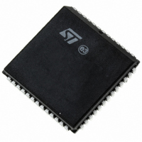
PSD813F1A-90JI STMicroelectronics, PSD813F1A-90JI Datasheet - Page 69

PSD813F1A-90JI
Manufacturer Part Number
PSD813F1A-90JI
Description
IC FLASH 1MBIT 90NS 52PLCC
Manufacturer
STMicroelectronics
Datasheet
1.PSD813F1A-90U.pdf
(111 pages)
Specifications of PSD813F1A-90JI
Format - Memory
FLASH
Memory Type
FLASH
Memory Size
1M (128K x 8)
Speed
90ns
Interface
Parallel
Voltage - Supply
4.5 V ~ 5.5 V
Operating Temperature
-40°C ~ 85°C
Package / Case
52-PLCC
Lead Free Status / RoHS Status
Contains lead / RoHS non-compliant
Other names
497-1976-5
Available stocks
Company
Part Number
Manufacturer
Quantity
Price
Company:
Part Number:
PSD813F1A-90JI
Manufacturer:
WSI
Quantity:
10
Company:
Part Number:
PSD813F1A-90JI
Manufacturer:
STMicroelectronics
Quantity:
10 000
RESET TIMING AND DEVICE STATUS AT RESET
Power-On Reset
Upon Power-up, the PSD requires a Reset (RE-
SET) pulse of duration t
and
period, the device loads internal configurations,
clears some of the registers and sets the Flash
memory or EEPROM into Operating mode. After
the rising edge of Reset (RESET), the PSD re-
mains in the Reset mode for an additional period,
t
first memory access is allowed.
The PSD Flash or EEPROM memory is reset to
the READ mode upon power up. The FSi and
EESi select signals along with the write strobe sig-
nal must be in the false state during power-up re-
set for maximum security of the data contents and
to remove the possibility of a byte being written on
the first edge of a write strobe signal. The PSD au-
tomatically prevents write strobes from reaching
the EEPROM memory array for about 5ms (t
WL
prevented automatically when V
Figure 35. Reset (RESET) Timing
OPR
). Any Flash memory WRITE cycle initiation is
68
V
RESET
(See Tables
CC
for values) after V
67
and
Power-On Reset
V
t NLNH-PO
CC
NLNH-PO
68
CC
(min)
for values), before the
is steady. During this
CC
(See Tables
is below V
t OPR
EEH-
LKO
67
.
Warm Reset
Once the device is up and running, the device can
be reset with a much shorter pulse of t
Tables
is needed before the device is operational after
warm reset. Figure
power on and warm reset.
I/O Pin, Register and PLD Status at Reset
Table 33., page 70
PLD status during Power On Reset, Warm reset
and Power-down mode. PLD outputs are always
valid during warm reset, and they are valid in Pow-
er On Reset once the internal PSD Configuration
bits are loaded. This loading of PSD is completed
typically long before the V
ing level. Once the PLD is active, the state of the
outputs are determined by the PSDabel equa-
tions.
67
and
68
for values). The same t
shows the I/O pin, register and
Warm Reset
t NLNH-A
35
t NLNH
shows the timing of the
CC
ramps up to operat-
PSD813F1A
t OPR
AI02866b
NLNH
OPR
69/111
(See
time


