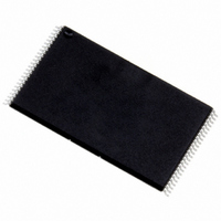
NAND128W3A0AN6 STMicroelectronics, NAND128W3A0AN6 Datasheet - Page 28

NAND128W3A0AN6
Manufacturer Part Number
NAND128W3A0AN6
Description
IC FLASH 128MBIT 48TSOP
Manufacturer
STMicroelectronics
Datasheet
1.NAND128W3A2BN6E.pdf
(56 pages)
Specifications of NAND128W3A0AN6
Format - Memory
FLASH
Memory Type
FLASH - Nand
Memory Size
128M (16M x 8)
Interface
Parallel
Voltage - Supply
2.7 V ~ 3.6 V
Operating Temperature
-40°C ~ 85°C
Package / Case
48-TSOP
Lead Free Status / RoHS Status
Lead free / RoHS Compliant
Speed
-
Available stocks
Company
Part Number
Manufacturer
Quantity
Price
Company:
Part Number:
NAND128W3A0AN6
Manufacturer:
ST
Quantity:
4 000
Part Number:
NAND128W3A0AN6E
Manufacturer:
ST
Quantity:
20 000
NAND128-A, NAND256-A, NAND512-A, NAND01G-A
Automatic Page 0 Read at Power-Up
Automatic Page 0 Read at Power-Up is an option
available on all devices belonging to the NAND
Flash 528 Byte/264 Word Page family. It allows
the microcontroller to directly download boot code
from page 0, without requiring any command or
address input sequence. The Automatic Page 0
Read option is particularly suited for applications
that boot from the NAND.
Devices delivered with Automatic Page 0 Read at
Power-Up can have the Chip Enable Don’t Care
option either enabled or disabled. For details on
how to order the different options, refer to
28., Ordering Information
Automatic Page 0 Read Description. At power-
up, once the supply voltage has reached the
threshold level, V
their reset state and the internal NAND device
functions (reading, writing, erasing) are enabled.
The device then automatically switches to read
mode where, as in any read operation, the device
is busy for a time t
ferred to the Page Buffer. Once the data transfer is
Figure 20. Chip Enable Don’t Care Enabled and Automatic Page 0 Read at Power-Up
Note: 1.
28/56
V
V
DDth
RB
I/O
AL
CL
V
DD
W
E
R
DD
(1)
th
is equal to 2.5V for 3V Power Supply devices and to 1.5V for 1.8V Power Supply devices.
BLBH1
DDth
, all digital outputs revert to
during which data is trans-
Scheme.
Busy
tBLBH1
from Address N to Last Byte or Word in Page
Data
N
Table
Data
N+1
Data Output
complete the Ready/Busy signal goes High. The
data can then be read out sequentially on the I/O
bus by pulsing the Read Enable, R, signal.
20.
for devices featuring the Automatic Page 0 Read
option.
Chip Enable Don’t Care Enabled. If the device
is delivered with Chip Enable Don’t Care and Au-
tomatic Page 0 Read at Power-up, only the first
page (Page 0) will be automatically read after the
power-up sequence. Refer to
Chip Enable Don’t Care Disabled. If the device
is delivered with the Automatic Page 0 Read op-
tion only (Chip Enable Don’t Care disabled), the
device will automatically enter Sequential Row
Read mode (Automatic Memory Download) after
the power-up sequence, and start reading Page 0,
Page 1, etc., until the last memory location is
reached, each new page being accessed after a
time t
The Sequential Row Read operation can be inhib-
ited or interrupted by de-asserting E (set to V
by issuing a command.
Data
N+2
and
BLBH1
Figure 21.
.
Data
Last
show the power-up waveforms
Figure
20..
ai08443b
Figure
IH
) or


