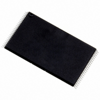
NAND256W3A2BN6F STMicroelectronics, NAND256W3A2BN6F Datasheet - Page 55

NAND256W3A2BN6F
Manufacturer Part Number
NAND256W3A2BN6F
Description
IC FLASH 256MBIT 48TSOP
Manufacturer
STMicroelectronics
Datasheet
1.NAND128W3A2BN6E.pdf
(59 pages)
Specifications of NAND256W3A2BN6F
Format - Memory
FLASH
Memory Type
FLASH - Nand
Memory Size
256M (32M x 8)
Interface
Parallel
Voltage - Supply
2.7 V ~ 3.6 V
Operating Temperature
-40°C ~ 85°C
Package / Case
48-TSOP
Lead Free Status / RoHS Status
Lead free / RoHS Compliant
Speed
-
Available stocks
Company
Part Number
Manufacturer
Quantity
Price
Company:
Part Number:
NAND256W3A2BN6F
Manufacturer:
ST
Quantity:
4 000
Part Number:
NAND256W3A2BN6F
Manufacturer:
ST
Quantity:
20 000
NAND128-A, NAND256-A
Appendix A
NAND flash devices can be connected to a microcontroller system bus for code and data
storage. For microcontrollers that have an embedded NAND controller the NAND flash can
be connected without the addition of glue logic (see
logic is required for general purpose microcontrollers that do not have an embedded NAND
controller. The glue logic usually consists of a flip-flop to hold the Chip Enable, Address
Latch Enable, and Command Latch Enable signals stable during command and address
latch operations, and some logic gates to simplify the firmware or make the design more
robust.
Figure 39
microcontroller. The additional OR gates allow the microcontroller’s Output Enable and
Write Enable signals to be used for other peripherals. The OR gate between A3 and CSn
maps the flip-flop and NAND I/O in different address spaces inside the same chip select
unit, which improves the setup and hold times and simplifies the firmware. The structure
uses the microcontroller DMA (direct memory access) engines to optimize the transfer
between the NAND flash and the system RAM.
For any interface with glue logic, the extra delay caused by the gates and flip-flop must be
taken into account. This delay must be added to the microcontroller’s AC characteristics and
register settings to get the NAND flash setup and hold times.
For mass storage applications (hard disk emulations or systems where a huge amount of
storage is required) NAND flash memories can be connected together to build storage
modules (see
Figure 38. Connection to microcontroller, without glue logic
Microcontroller
provides an example of how to connect a NAND flash to a general purpose
Hardware interface examples
Figure
AD(24:16)
PWAITEN
CSn
DQ
40).
G
W
V DD or V SS
or General Purpose I/O
AD17
AD16
Figure
V DD
38). However, a minimum of glue
Hardware interface examples
AL
CL
R
W
E
I/O
RB
WP
NAND
Flash
AI08045b
55/59


