EPC1213LC20 Altera, EPC1213LC20 Datasheet - Page 68
EPC1213LC20
Manufacturer Part Number
EPC1213LC20
Description
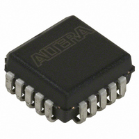
IC CONFIG DEVICE 212KBIT 20-PLCC
Manufacturer
Altera
Series
EPCr
Datasheet
1.EPC4QI100N.pdf
(116 pages)
Specifications of EPC1213LC20
Programmable Type
OTP
Memory Size
212kb
Voltage - Supply
4.75 V ~ 5.25 V
Operating Temperature
0°C ~ 70°C
Package / Case
20-PLCC
For Use With
PLMJ1213 - PROGRAMMER ADAPTER 20 PIN J-LEAD
Lead Free Status / RoHS Status
Contains lead / RoHS non-compliant
Other names
544-2188-5
Available stocks
Company
Part Number
Manufacturer
Quantity
Price
Company:

Part Number:
EPC1213LC20
Manufacturer:
AT
Quantity:
23
Company:
Part Number:
EPC1213LC20
Manufacturer:
ALTERA
Quantity:
5 510
Company:
Part Number:
EPC1213LC20
Manufacturer:
TI
Quantity:
5 510
Part Number:
EPC1213LC20
Manufacturer:
ALTERA/阿尔特拉
Quantity:
20 000


3–16
Configuration Handbook (Complete Two-Volume Set)
Write Disable Operation
The write disable operation code is b'0000 0100, with the MSB listed first. The
write disable operation resets the write enable latch bit, which is bit 1 in the status
register. To prevent the memory from being written unintentionally, the write enable
latch bit is automatically reset when implementing the write disable operation as well
as under the following conditions:
■
■
■
■
■
Figure 3–6
Figure 3–6. Write Disable Operation Timing Diagram
Read Status Operation
The read status operation code is b'0000 0101, with the MSB listed first. You can
use the read status operation to read the status register.
show the status bits in the status register of the serial configuration devices.
Figure 3–7. EPCS4, EPCS16, EPCS64, and EPCS128 Status Register Status Bits
Figure 3–8. EPCS1 Status Register Status Bits
Setting the write in progress bit to 1 indicates that the serial configuration device is
busy with a write or erase cycle. Resetting the write in progress bit to 0 means no
write or erase cycle is in progress.
Power up
Write bytes operation completion
Write status operation completion
Erase bulk operation completion
Erase sector operation completion
shows the timing diagram for the write disable operation.
Chapter 3: Serial Configuration Devices (EPCS1, EPCS4, EPCS16, EPCS64, and EPCS128) Data Sheet
DCLK
DATA
ASDI
nCS
Bit 7
Bit 7
High Impedance
0
1
BP2
Block Protect Bits [2..0]
2
Operation Code
BP1
BP1
Block Protect
3
Bits [1..0]
4
BP0
BP0
5
Write Enable
Write Enable
Latch Bit
Latch Bit
WEL
WEL
6
Serial Configuration Device Memory Access
Progress Bit
Progress Bit
7
Figure 3–7
Write In
Write In
WIP
Bit 0
WIP
Bit 0
© December 2009
and
Figure 3–8
Altera Corporation
Related parts for EPC1213LC20
Image
Part Number
Description
Manufacturer
Datasheet
Request
R

Part Number:
Description:
CUSTOMER ADVISORY EPC1064 and EPC1213 Transition Schedule Update
Manufacturer:
Altera Corporation
Part Number:
Description:
Configuration EPROMs For Flex Devices
Manufacturer:
Altera Corporation
Datasheet:

Part Number:
Description:
CYCLONE II STARTER KIT EP2C20N
Manufacturer:
Altera
Datasheet:

Part Number:
Description:
CPLD, EP610 Family, ECMOS Process, 300 Gates, 16 Macro Cells, 16 Reg., 16 User I/Os, 5V Supply, 35 Speed Grade, 24DIP
Manufacturer:
Altera Corporation
Datasheet:
Part Number:
Description:
CPLD, EP610 Family, ECMOS Process, 300 Gates, 16 Macro Cells, 16 Reg., 16 User I/Os, 5V Supply, 15 Speed Grade, 24DIP
Manufacturer:
Altera Corporation
Datasheet:
Part Number:
Description:
Manufacturer:
Altera Corporation
Datasheet:
Part Number:
Description:
CPLD, EP610 Family, ECMOS Process, 300 Gates, 16 Macro Cells, 16 Reg., 16 User I/Os, 5V Supply, 30 Speed Grade, 24DIP
Manufacturer:
Altera Corporation
Datasheet:
Part Number:
Description:
High-performance, low-power erasable programmable logic devices with 8 macrocells, 10ns
Manufacturer:
Altera Corporation
Datasheet:
Part Number:
Description:
High-performance, low-power erasable programmable logic devices with 8 macrocells, 7ns
Manufacturer:
Altera Corporation
Datasheet:
Part Number:
Description:
Classic EPLD
Manufacturer:
Altera Corporation
Datasheet:
Part Number:
Description:
High-performance, low-power erasable programmable logic devices with 8 macrocells, 10ns
Manufacturer:
Altera Corporation
Datasheet:
Part Number:
Description:
Manufacturer:
Altera Corporation
Datasheet:
Part Number:
Description:
Manufacturer:
Altera Corporation
Datasheet: