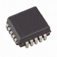
AT17C020A-10JI Atmel, AT17C020A-10JI Datasheet - Page 2

AT17C020A-10JI
Manufacturer Part Number
AT17C020A-10JI
Description
IC SERIAL CONFIG PROM 2M 20PLCC
Manufacturer
Atmel
Datasheet
1.AT17C020A-10JC.pdf
(13 pages)
Specifications of AT17C020A-10JI
Programmable Type
Serial EEPROM
Memory Size
2Mb
Voltage - Supply
4.5 V ~ 5.5 V
Operating Temperature
-40°C ~ 85°C
Package / Case
20-LCC (J-Lead)
Lead Free Status / RoHS Status
Contains lead / RoHS non-compliant
Other names
AT17C020A10JI
Available stocks
Company
Part Number
Manufacturer
Quantity
Price
Block Diagram
Device Configuration
The control signals for the configuration EEPROM-nCS,
OE, and DCLK-interface directly with the FPGA device
control signals. All FPGA devices can control the entire
configuration process and retrieve data from the configura-
tion EEPROM without requiring an external intelligent
controller.
The configuration EEPROM’s OE and nCS pins control the
tri-state buffer on the DATA output pin and enable the
address counter and the oscillator. When OE is driven Low,
the configuration EEPROM resets its address counter and
tri-states its DATA pin. The nCS pin also controls the out-
put of the AT17A Series Configurator. If nCS is held High
after the OE reset pulse, the counter is disabled and the
DATA output pin is tri-stated. When nCS is driven Low, the
counter and the DATA output pin are enabled. When OE is
2
POWER ON
CONTROL
RESET
OSC
OSC
SER_EN
DCLK READY
AT17C/LV020A
PROGRAMMING
COUNTER
COUNTER
ADDRESS
MODE LOGIC
ROW
BIT
OE
driven Low again, the address counter is reset and
the DATA output pin is tri-stated, regardless of the state
of the nCS.
When the Configurator has driven out all of its data and
nCASC is driven Low, the device tri-states the DATA pin to
avoid contention with other Configurators. Upon power-up,
the address counter is automatically reset.
The READY pin is available as an open-collector indicator
of the device’s reset status; it is driven Low while the device
is in its power-on reset cycle and released (tri-stated) when
the cycle is complete.
This document discusses the EPF10K device interface.
For more details or information on other Altera applications,
please reference the “AT17A Series Conversions from
Altera FPGA Serial Configuration Memories” application
note.
nCS
DECODER
ROW
TC
nCASC (A2)
PROGRAMMING
DECODER
COLUMN
DATA SHIFT
REGISTER
EEPROM
MATRIX
CELL
DATA


