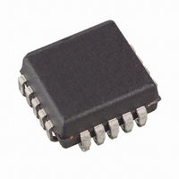
AT17C020A-10JI Atmel, AT17C020A-10JI Datasheet - Page 3

AT17C020A-10JI
Manufacturer Part Number
AT17C020A-10JI
Description
IC SERIAL CONFIG PROM 2M 20PLCC
Manufacturer
Atmel
Datasheet
1.AT17C020A-10JC.pdf
(13 pages)
Specifications of AT17C020A-10JI
Programmable Type
Serial EEPROM
Memory Size
2Mb
Voltage - Supply
4.5 V ~ 5.5 V
Operating Temperature
-40°C ~ 85°C
Package / Case
20-LCC (J-Lead)
Lead Free Status / RoHS Status
Contains lead / RoHS non-compliant
Other names
AT17C020A10JI
Available stocks
Company
Part Number
Manufacturer
Quantity
Price
FPGA Device Configuration
FPGA devices can be configured with an AT17A Series
EEPROM as shown in Figure 1. The AT17A Series device
stores configuration data in its EEPROM array and clocks
the data out serially with its internal oscillator. The OE,
nCS, and DCLK pins supply the control signals for the
address counter and the output tri-state buffer. The AT17A
Series device sends a serial bitstream of configuration data
to its DATA pin, which is connected to the DATA0 input pin
on the FPGA device.
When configuration data for an FPGA device exceeds the
capacity of a single AT17A Series device, multiple AT17A
Series devices can be serially linked together (Figure 2).
When multiple AT17A Series devices are required, the
nCASC and nCS pins provide handshaking between the
cascaded EEPROMs.
The position of an AT17A Series device in a chain deter-
mines its operation. The first AT17A Series device in a
Configurator chain is powered up or reset with nCS Low
and is configured for the FPGA device’s protocol. This
AT17A Series device supplies all clock pulses to one or
more FPGA devices and to any downstream AT17A Series
Configurator during configuration. The first AT17A Series
Configurator also provides the first stream of data to the
FPGA devices during multi-device configuration. Once the
Figure 1. Configuration with a Single AT17A Series Configurator
Notes:
1. 1.0 kΩ resistors used unless otherwise specified.
2. Applicable to EPF6K.
3. Use of the READY pin is optional.
4. Introducing a RC delay to the input of nCONFIG is recommended to ensure that V
5. Reset polarity of EEPROM must be set active Low (OE active High).
configuration begins. (nCONFIG can instead be connected to an active Low system reset signal.)
VCC
GND
nCONFIG
nCE
MSEL0
MSEL1
EPF10K
CONF_DONE
nSTATUS
DATA0
DCLK
VCC
first AT17A Series device finishes sending configuration
data, it drives its nCASC pin Low, which drives the nCS pin
of the second AT17A Series device Low. This activates the
second AT17A Series device to send configuration data to
the FPGA device.
The first AT17A Series device clocks all subsequent
AT17A Series devices until configuration is complete. Once
all configuration data is transferred and nCS on the first
AT17A Series device is driven High by CONF_DONE on
the FPGA devices, the first AT17A Series device clocks 16
additional cycles to initialize the FPGA device before going
into zero-power (idle) state. If nCS on the first AT17A
Series device is driven High before all configuration data is
transferred – or if the nCS is not driven High after all config-
uration data is transferred – nSTATUS is driven Low,
indicating a configuration error.
The READY pin is available as an open-collector indicator
of the device’s reset status; it is driven Low while the device
is in its power-on reset cycle and released (tri-stated) when
the cycle is complete. It can be used to hold the FPGA
device in reset while it is completing its power-on reset but
it cannot be used to effectively delay configuration (i.e., the
output is released well before the system V
stabilized).
VCC
AT17LV512A/010A/020A
AT17C512A/010A/020A
CC
DCLK
DATA
nCS
OE
(5V/3.3V) is reached before
READY
C C
has
3


