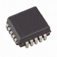
AT17C020A-10JI Atmel, AT17C020A-10JI Datasheet - Page 5

AT17C020A-10JI
Manufacturer Part Number
AT17C020A-10JI
Description
IC SERIAL CONFIG PROM 2M 20PLCC
Manufacturer
Atmel
Datasheet
1.AT17C020A-10JC.pdf
(13 pages)
Specifications of AT17C020A-10JI
Programmable Type
Serial EEPROM
Memory Size
2Mb
Voltage - Supply
4.5 V ~ 5.5 V
Operating Temperature
-40°C ~ 85°C
Package / Case
20-LCC (J-Lead)
Lead Free Status / RoHS Status
Contains lead / RoHS non-compliant
Other names
AT17C020A10JI
Available stocks
Company
Part Number
Manufacturer
Quantity
Price
Pin Configurations
Absolute Maximum Ratings*
Operating Temperature.................................. -55°C to +125°C
Storage Temperature ..................................... -65°C to +150°C
Voltage on Any Pin
with Respect to Ground ..............................-0.1V to V
Supply Voltage (V
Maximum Soldering Temp. (10 sec @ 1/16 in.)..............260°C
ESD (R
PLCC
Pin
20
10
12
15
18
20
2
4
8
9
ZAP
SER_EN
nCASC
READY
Name
DCLK
DATA
GND
VCC
= 1.5K, C
nCS
OE
A2
CC
) .........................................-0.5V to +7.0V
ZAP
I/O
I/O
I/O
O
O
I
I
I
I
= 100 pF) ................................ 2000V
Description
Three-state data output for configuration. Open-collector bi-directional pin for programming.
Clock output or clock input. Rising edges on DCLK increment the internal address counter and present the
next bit of data to the DATA pin. The counter is incremented only if the OE input is held High, the nCS input
is held Low, and all configuration data has not been transferred to the target device (otherwise, as the
master device, the DCLK pin drives Low).
Output enable (active High) and reset (active Low) when SER_EN is High. A Low logic level resets the
address counter. A High logic level (with nCS Low) enables DATA and permits the address counter to
count. In the mode, if this pin is Low (reset), the internal oscillator becomes inactive and DCLK drives Low.
The logic polarity of this input is programmable and must be programmed active High (RESET active Low)
by the user during programming for Altera applications.
Chip select input (active Low). A Low input (with OE High) allows DCLK to increment the address counter
and enables DATA to drive out. If the AT17A Series is reset with nCS Low, the device initializes as the first
(and master) device in a daisy-chain. If the AT17A Series is reset with nCS High, the device initializes as a
subsequent AT17A Series device in the chain.
Ground pin. A 0.2 µF decoupling capacitor should be placed between the VCC and GND pins.
Cascade select output (active Low). This output goes Low when the address counter has reached its
maximum value. In a daisy-chain of AT17A Series devices, the nCASC pin of one device is usually
connected to the nCS input pin of the next device in the chain, which permits DCLK from the master
Configurator to clock data from a subsequent AT17A Series device in the chain.
Device selection input, A2. This is used to enable (or select) the device during programming, (i.e., when
SER_EN is Low; please refer to the “Programming Specification” application note for more details).
Open collector reset state indicator. Driven Low during power-up reset, released (tri-stated) when
power-up is complete. (Recommend a 4.7 kΩ pull-up on this pin if used).
Serial enable must be held High during FPGA loading operations. Bringing SER_EN Low, enables the
2-wire serial programming mode.
+3.3V/+5V power supply pin
CC
+0.5V
*NOTICE:
Stresses beyond those listed under Absolute Maxi-
mum Ratings may cause permanent damage to the
device. These are stress ratings only, and functional
operation of the device at these or any other condi-
tions beyond those listed under Operating Conditions
is not implied. Exposure to Absolute Maximum
Ratings conditions for extended periods of time
may affect device reliability.
5


