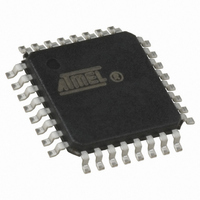
AT17C002A-10QI Atmel, AT17C002A-10QI Datasheet - Page 3

AT17C002A-10QI
Manufacturer Part Number
AT17C002A-10QI
Description
IC SRL CONFIG EEPROM 2M 32TQFP
Manufacturer
Atmel
Datasheet
1.AT17C002A-10JC.pdf
(14 pages)
Specifications of AT17C002A-10QI
Programmable Type
Serial EEPROM
Memory Size
2Mb
Voltage - Supply
4.5 V ~ 5.5 V
Operating Temperature
-40°C ~ 85°C
Package / Case
32-TQFP
Lead Free Status / RoHS Status
Contains lead / RoHS non-compliant
Device
Configuration
FPGA Device
Configuration
2280B–08/01
The control signals for the configuration EEPROM (nCS, OE and DCLK) interface directly with
the FPGA device control signals. All FPGA devices can control the entire configuration pro-
cess and retrieve data from the configuration EEPROM without requiring an external intelligent
controller.
The configuration EEPROM’s OE and nCS pins control the tri-state buffer on the DATA output
pin and enable the address counter and the oscillator. When OE is driven Low, the configura-
tion EEPROM resets its address counter and tri-states its DATA pin. The nCS pin also
controls the output of the AT17A Series Configurator. If nCS is held High after the OE reset
pulse, the counter is disabled and the DATA output pin is tri-stated. When nCS is driven Low,
the counter and the DATA output pin are enabled. When OE is driven Low again, the address
counter is reset and the DATA output pin is tri-stated, regardless of the state of the nCS.
When the Configurator has driven out all of its data and nCASC is driven Low, the device tri-
states the DATA pin to avoid contention with other Configurators. Upon power-up, the address
counter is automatically reset.
The READY pin is available as an open-collector indicator of the device’s reset status; it is
driven Low while the device is in its power-on reset cycle and released (tri-stated) when the
cycle is complete.
This document discusses the EPF10K device interface. For more details or information on
other Altera applications, please reference the “AT17A Series Conversions from Altera FPGA
Serial Configuration Memories” application note.
FPGA devices can be configured with an AT17A Series EEPROM (see Figure 1). The AT17A
Series device stores configuration data in its EEPROM array and clocks the data out serially
with its internal oscillator. The OE, nCS and DCLK pins supply the control signals for the
address counter and the output tri-state buffer. The AT17A Series device sends a serial bit-
stream of configuration data to its DATA pin, which is connected to the DATA0 input pin on the
FPGA device.
When the configuration data for an FPGA device exceeds the capacity of a single AT17A
Series device, multiple AT17A Series devices can be serially linked together (see Figure 2).
When multiple AT17A Series devices are required, the nCASC and nCS pins provide hand-
shaking between the cascaded EEPROMs.
The position of an AT17A Series device in a chain determines its operation. The first AT17A
Series device in a configurator chain is powered up or reset with nCS Low and is configured
for the FPGA device’s protocol. This AT17A Series device supplies all clock pulses to one or
more FPGA devices and to any downstream AT17A Series Configurator during configuration.
The first AT17A Series Configurator also provides the first stream of data to the FPGA devices
during multi-device configuration. Once the first AT17A Series device finishes sending config-
uration data, it drives its nCASC pin Low, which drives the nCS pin of the second AT17A
Series device Low. This activates the second AT17A Series device to send configuration data
to the FPGA device.
3


