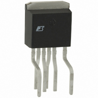
PKS606FN Power Integrations, PKS606FN Datasheet - Page 11

PKS606FN
Manufacturer Part Number
PKS606FN
Description
IC OFFLINE SWIT OTP OCP HV TO262
Manufacturer
Power Integrations
Series
PeakSwitch®r
Specifications of PKS606FN
Mfg Application Notes
PeakSwitch Design Guide AppNote
Output Isolation
Isolated
Frequency Range
250 ~ 304kHz
Voltage - Output
700V
Power (watts)
117W
Operating Temperature
-40°C ~ 150°C
Package / Case
TO-262-7 (Formed Leads), 5 Leads
Output Voltage
12 V
Input / Supply Voltage (max)
265 VAC
Input / Supply Voltage (min)
85 VAC
Duty Cycle (max)
65 %
Switching Frequency
47 KHz
Supply Current
25 uA
Operating Temperature Range
- 40 C to + 150 C
Mounting Style
Through Hole
For Use With
596-1198 - KIT REF DESIGN 36-72W MOTOR DRVR
Lead Free Status / RoHS Status
Lead free / RoHS Compliant
Other names
596-1125-5
Available stocks
Company
Part Number
Manufacturer
Quantity
Price
Company:
Part Number:
PKS606FN
Manufacturer:
power
Quantity:
15 000
Part Number:
PKS606FN
Manufacturer:
POWER
Quantity:
20 000
race conditions that could cause unwanted triggering during
brownout or on removal of the AC input.
Referring to Figure 1, the fast AC reset circuit is comprised
of D5, C7, R5 and R6. The incoming AC is rectified by D5
and filtered by C7 with R5 and R6 providing the line sensing
current into the EN/UV pin. When AC power is removed (after
a fault has occurred and the unit has latched off), C7 discharges
quickly via R5 and R6. The value of C7 is selected so that the
current through R5 and R6 has fallen below the UV threshold
(25 µA) after the desired reset time (~3 seconds as shown) has
elapsed. The capacitor should have a voltage rating greater
than VAC
suitable choice.
If the line UVLO function and latching shutdown are desired
and fast AC reset is not required, then the resistor value from
step 3 can be connected from the UV/EN pin to the positive
side of the input bulk capacitor.
If no resistors are fitted then the PeakSwitch device senses this
condition and the UVLO function is disabled.
The sense resistor should be rated above 400 V, generally
requiring either a single 0.5 W resistor or two 0.25 W resistors
connected in series.
Table 4. List of Diodes Suitable For Use as the Output Rectifier.
IN5817 to 1N5819
SB120 to SB1100
11DQ50 to 11DQ60
1N5820 to 1N5822
MBR320 to MBR360
SS12 to SS16
SS32 to SS36
SB540 to SB560
UF4002 to UF4006
MUR110 to MUR160
UF5401 to UF5408
ES1A to ES1D
ES2A to ES2D
BYV28-200
MBR745 to MBR760
MBR1045 to MBR10100
BYW29-100 to BYW29-200
MAX
Series Number
× √2, with 400 V metal film capacitors being a
Schottky
Schottky
Schottky
Schottky
Schottky
Schottky
Schottky
Schottky
Ultrafast
Ultrafast
Ultrafast
Ultrafast
Ultrafast
Ultrafast
Schottky
Schottky
Ultrafast
Type
20-40
20-100
50-60
20-40
20-60
20-60
20-60
40-60
100-600
100-600
100-800
50-200
50-200
200
40-60
45-100
100-200
V
R
Range
V
Step – Selection of Primary Clamp Components
It is recommended that either a Zener clamp or an RCD combined
with a Zener clamp be used in PeakSwitch designs. This is to
ensure that the peak drain voltage is limited to below the BV
of the internal MOSFET while still maximizing efficiency and
minimizing no-load consumption.
A standard RCD clamp designed to limit the peak drain voltage
under peak load conditions represents a significant load as the
output power is reduced, resulting in low light load efficiency
and high no-load consumption.
Figure 1 shows an example of an optimized clamp arrangement.
The addition of VR1 in series with R3 prevents C5 from
discharging below 100 V as the effective switching frequency
lowers as the load is reduced. The value of R3 is selected so
that the peak drain voltage is limited to an acceptable level under
worst-case conditions of maximum input voltage, maximum
ambient temperature and maximum overload power or a short
circuit on the output of the supply.
The peak drain voltage should be limited to a maximum voltage
of 650 V under these conditions to provide margin for component
variation. In the sample design shown in these steps, the peak
drain voltage was limited to 600 V. The clamp diode (D6) must
3.5
7.5
10
I
A
1
1
1
3
3
1
3
5
1
1
3
1
2
8
D
Leaded
Leaded
Leaded
Leaded
Leaded
SMD
SMD
Leaded
Leaded
Leaded
Leaded
SMD
SMD
Leaded
TO220
TO220
TO220
Package
Vishay
Vishay/Fairchild
IR
Vishay
IR/On Semi
Vishay
Vishay
Vishay
Vishay
On Semi
Vishay
Vishay
Vishay
Vishay
Vishay
Vishay
Vishay
Manufacturer
AN-41
Rev. E 02/07
11
DSS


