TOP234GN Power Integrations, TOP234GN Datasheet - Page 20
TOP234GN
Manufacturer Part Number
TOP234GN
Description
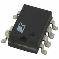
IC OFFLINE SWIT OVP UVLO 8SMD
Manufacturer
Power Integrations
Series
TOPSwitch®-FXr
Type
Off Line Switcherr
Datasheet
1.TOP234YN.pdf
(36 pages)
Specifications of TOP234GN
Output Isolation
Isolated
Frequency Range
66 ~ 132kHz
Voltage - Output
700V
Power (watts)
30W
Operating Temperature
-40°C ~ 150°C
Package / Case
8-SMD Gull Wing, 7 Leads
Output Voltage
12 V
Input / Supply Voltage (max)
265 VAC
Input / Supply Voltage (min)
85 VAC
Duty Cycle (max)
78 %
Switching Frequency
132 KHz
Supply Current
1.5 mA
Operating Temperature Range
- 40 C to + 150 C
Mounting Style
SMD/SMT
Lead Free Status / RoHS Status
Lead free / RoHS Compliant
Available stocks
Company
Part Number
Manufacturer
Quantity
Price
Company:

Part Number:
TOP234GN
Manufacturer:
PowerInt
Quantity:
350
Part Number:
TOP234GN
Manufacturer:
POWER
Quantity:
20 000
Part Number:
TOP234GN-TL
Manufacturer:
POWER
Quantity:
20 000


*Not available
Table 3 (cont). Comparison Between TOPSwitch-II and TOPSwitch-FX.
TOPSwitch-FX Design Considerations
TOPSwitch-FX Selection
Selecting the optimum TOPSwitch-FX depends upon required
maximum output power, efficiency, heat sinking constraints
and cost goals. With the option to externally reduce current
limit, a larger TOPSwitch-FX may be used for lower power
applications where higher efficiency is needed or minimal heat
sinking is available.
Input Capacitor
The input capacitor must be chosen to provide the minimum
DC voltage required for the TOPSwitch-FX converter to maintain
regulation at the lowest specified input voltage and maximum
output power. Since TOPSwitch-FX has a higher DC
TOPSwitch-II, it is possible to use a smaller input capacitor. For
TOPSwitch-FX, a capacitance of 2 µF per watt is usually
sufficient for universal input with an appropriately designed
transformer.
20
Function
Remote ON/OFF
Synchronization
Thermal Shutdown
Current Limit Tolerance ±10% (@25 °C)
DRAIN
Creepage at
Package
DRAIN Creepage at
PCB for TO-220
TOP232-234
B
7/01
DIP
SMD
TO-220 0.046" / 1.17 mm
TOPSwitch-II
N/A*
N/A*
Latched
-8% (0 °C to100 °C) -4% (0 °C to 100 °C)
0.037" / 0.94 mm
0.037" / 0.94 mm
0.045" / 1.14 mm
TOPSwitch-FX
±7% (@25 °C)
(preformed leads)
Single transistor
or optocoupler
interface or manual 22, 23, • Low consumption in remote off state
switch
Single transistor
or optocoupler
interface
Hysteretic (with
70 °C hysteresis)
0.137" / 3.48 mm
0.137" / 3.48 mm
0.068" / 1.73 mm
0.113" / 2.87 mm
MAX
than
Primary Clamp and Output Reflected Voltage V
A primary clamp is necessary to limit the peak TOPSwitch-FX
drain to source voltage. A Zener clamp (see Figure 26, VR1)
requires few parts and takes up little board space. For good
efficiency, the clamp Zener should be selected to be at least 1.5
times the output reflected voltage V
spike conduction time short. When using a Zener clamp in a
universal input application, a V
recommended to allow for the absolute tolerances and
temperature variations of the Zener. This will ensure efficient
operation of the clamp circuit and will also keep the maximum
drain voltage below the rated breakdown voltage of the
TOPSwitch-FX MOSFET.
A high V
of TOPSwitch-FX. An RCD clamp provides tighter clamp
voltage tolerance than a Zener clamp and allows a V
as 165 V. The V
designs up to 185 V by reducing the external current limit as a
function of input line voltage (see Figure 18). The RCD clamp
Figures Advantages
8, 19,
20, 21, • Active-on or active-off control
27
OR
is required to take full advantage of the wider DC
OR
• Fast on/off (cycle by cycle)
• Active-on control for fail-safe
• Eliminates expensive in-line on/off
• Allows processor controlled turn on/
• Permits shutdown/wake-up of
• Synchronization to external lower
• Starts new switching cycle on
• Automatic recovery from thermal
• Large hysteresis prevents circuit
• 10% higher power capability due to
• Greater immunity to arcing as a
• Preformed leads accommodate
• Easier to meet Safety (UL/VDE)
can be further increased in continuous mode
switch
off
peripherals via LAN or parallel port
frequency signal
demand
fault
board overheating
tighter tolerance
result of build-up of dust, debris and
other contaminants
large creepage for PCB layout
OR
OR
as this keeps the leakage
of less than 135 V is
OR
OR
as high
MAX
Related parts for TOP234GN
Image
Part Number
Description
Manufacturer
Datasheet
Request
R

Part Number:
Description:
SOP-16
Manufacturer:
Power Integrations
Datasheet:
Part Number:
Description:
DIP8
Manufacturer:
Power Integrations
Datasheet:
Part Number:
Description:
TO-263
Manufacturer:
Power Integrations
Datasheet:
Part Number:
Description:
TO-263
Manufacturer:
Power Integrations
Datasheet:
Part Number:
Description:
Manufacturer:
Power Integrations
Datasheet: