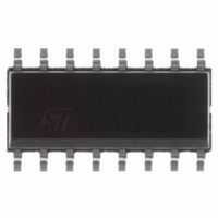
L6566B STMicroelectronics, L6566B Datasheet - Page 31

L6566B
Manufacturer Part Number
L6566B
Description
IC CTRLR OVP OTP UVLO HV 16SOIC
Manufacturer
STMicroelectronics
Datasheet
1.L6566BTR.pdf
(51 pages)
Specifications of L6566B
Output Isolation
Isolated
Frequency Range
10 ~ 300kHz
Voltage - Input
8 ~ 23 V
Power (watts)
750mW
Operating Temperature
-40°C ~ 150°C
Package / Case
16-SOIC (0.154", 3.90mm Width)
Output Current
800 mA
Output Power
750 mW
Input Voltage
8 V to 23 V
Operating Temperature Range
- 40 C to + 150 C
Mounting Style
SMD/SMT
Duty Cycle (max)
75 %
Selectable Multi-mode Operation
fixed frequency or quasi-resonant
For Use With
497-6452 - BOARD EVAL FOR L6566B497-6451 - BOARD EVAL FOR L6566B497-6450 - BOARD EVAL FOR L6566B497-6449 - BOARD EVAL FOR L6566A
Lead Free Status / RoHS Status
Lead free / RoHS Compliant
Available stocks
Company
Part Number
Manufacturer
Quantity
Price
Part Number:
L6566B
Manufacturer:
ST
Quantity:
20 000
Part Number:
L6566BHTR
Manufacturer:
ST
Quantity:
20 000
Part Number:
L6566BTR-13
Manufacturer:
ST
Quantity:
20 000
L6566B
5.8
between the detected event and the oscillator, occasionally the device could stop after the
third detection.
This condition is latched as long as the device is supplied. While it is disabled, however, no
energy is coming from the self-supply circuit; hence the voltage on the Vcc capacitor will
decay and cross the UVLO threshold after some time, which clears the latch. The internal
start-up generator is still off, then the Vcc voltage still needs to go below its restart voltage
before the Vcc capacitor is charged again and the device restarted. Ultimately, this will result
in a low-frequency intermittent operation (Hiccup-mode operation), with very low stress on
the power circuit. This special condition is illustrated in the timing diagram of
page 30
Frequency modulation
To alleviate converter’s EMI emissions and reduce cost and size of the line filter, it is
advantageous to modulate its switching frequency, so that the resulting spread-spectrum
action distributes the energy of each harmonic of the switching frequency over a number of
side-band harmonics. Their overall energy will be unchanged but the individual amplitudes
will be smaller. This is what naturally occurs with QR operation, due to the twice-mains-
frequency ripple appearing on the input bulk capacitor, which translates into different DCM-
CCM boundary frequencies.
The L6566B is provided with a dedicated pin, FMOD (6), to perform this function if FF mode
is selected.
Figure 19. Frequency modulation circuit
With reference to
alternately charged and discharged between 0.5 and 1.5 V by internal current generators
sourcing and sinking the same current (three times the current defined by the resistor R
pin OSC). Hence, the voltage across C
is determined by C
sourced by pin OSC will be modulated according a triangular profile at a frequency f
R
triangle will be little affected.
With this arrangement it is possible to set, nearly independently, the frequency deviation
Δf
MOD
sw
and the modulating frequency f
0 V
1 V
is considerably higher than R
.
Figure 19
MOD
. By connecting a resistor R
, the capacitor C
OSC
T
m
R
, as normally is, both f
T
, which define the modulation index:
MOD
13
L6566B
R
will be a symmetric triangle, whose frequency f
MOD
MOD
is connected from FMOD to ground and is
6
MOD
FMOD
C
MOD
from FMOD to OSC, the current
m
and the symmetry of the
Application information
Figure 18 on
1.5 V
0.5 V
m
. If
31/51
T
on
m


