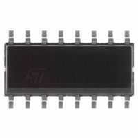
L6566B STMicroelectronics, L6566B Datasheet - Page 32

L6566B
Manufacturer Part Number
L6566B
Description
IC CTRLR OVP OTP UVLO HV 16SOIC
Manufacturer
STMicroelectronics
Datasheet
1.L6566BTR.pdf
(51 pages)
Specifications of L6566B
Output Isolation
Isolated
Frequency Range
10 ~ 300kHz
Voltage - Input
8 ~ 23 V
Power (watts)
750mW
Operating Temperature
-40°C ~ 150°C
Package / Case
16-SOIC (0.154", 3.90mm Width)
Output Current
800 mA
Output Power
750 mW
Input Voltage
8 V to 23 V
Operating Temperature Range
- 40 C to + 150 C
Mounting Style
SMD/SMT
Duty Cycle (max)
75 %
Selectable Multi-mode Operation
fixed frequency or quasi-resonant
For Use With
497-6452 - BOARD EVAL FOR L6566B497-6451 - BOARD EVAL FOR L6566B497-6450 - BOARD EVAL FOR L6566B497-6449 - BOARD EVAL FOR L6566A
Lead Free Status / RoHS Status
Lead free / RoHS Compliant
Available stocks
Company
Part Number
Manufacturer
Quantity
Price
Part Number:
L6566B
Manufacturer:
ST
Quantity:
20 000
Part Number:
L6566BHTR
Manufacturer:
ST
Quantity:
20 000
Part Number:
L6566BTR-13
Manufacturer:
ST
Quantity:
20 000
Application information
5.9
32/51
Equation 9
which is the parameter that the amplitude of the generated side-band harmonics depends
on.
The minimum frequency f
frequency f
around the centre value f
Equation 10
Then, R
oscillator block on page 21
Equation 11
where Δf
to achieve the best compromise between attenuation of peak EMI emissions and clean
converter operation.
Latched disable function
The device is equipped with a comparator having the non-inverting input externally available
at the pin DIS (8) and with the inverting input internally referenced to 4.5 V. As the voltage
on the pin exceeds the internal threshold, the device is immediately shut down and its
consumption reduced to a low value.
The information is latched and it is necessary to let the voltage on the Vcc pin go below the
UVLO threshold to reset the latch and restart the device. To keep the latch supplied as long
as the converter is connected to the input source, the HV generator is activated periodically
so that Vcc oscillates between the start-up threshold V
HV generator in this way cuts its power dissipation approximately by three (as compared to
the case of continuous conduction) and keeps peak silicon temperature close to the average
value.
To let the L6566B restart it is then necessary to disconnect the converter from the input
source. Pulling pin 16 (AC_OK) below the disable threshold (see
protection on page 37
latch can be cleared and a quicker restart is allowed as the input source is removed. This
operation is shown in the timing diagram of
T
sw
will be found from (5) (see
sw_max
and f
m
(occurring on the valley of the triangle) will be symmetrically placed
(in kHz, with C
) will stop the HV generator until Vcc falls below Vcc
f
sw
sw
_
sw_min
min
), while R
, so that:
R
MOD
=
f
sw
(occurring on the peak of the triangle) and the maximum
MOD
=
−
Section 5.2: Zero current detection and triggering block;
MOD
2
2
1
Δ
in nF and R
⋅
Δ
10
f
sw
f
sw
and C
β
3
;
=
Figure 20 on page 33
f Δ
f
m
MOD
sw
C
f
sw
MOD
MOD
_
can be calculated as follows:
max
ccON
in kΩ) will be selected by the user so
=
=
75
f
m
f
sw
and V
+
2
1
ccON
Section 5.12: Brownout
.
Δ
f
sw
- 0.5 V. Activating the
restart
, so that the
L6566B


