ADE7753ARSZ Analog Devices Inc, ADE7753ARSZ Datasheet - Page 34

ADE7753ARSZ
Manufacturer Part Number
ADE7753ARSZ
Description
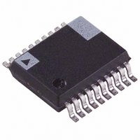
IC ENERGY METERING 1PHASE 20SSOP
Manufacturer
Analog Devices Inc
Datasheet
1.ADE7753ARSZ.pdf
(60 pages)
Specifications of ADE7753ARSZ
Input Impedance
390 KOhm
Measurement Error
0.1%
Voltage - I/o High
2.4V
Voltage - I/o Low
0.8V
Current - Supply
3mA
Voltage - Supply
4.75 V ~ 5.25 V
Operating Temperature
-40°C ~ 85°C
Mounting Type
Surface Mount
Package / Case
20-SSOP (0.200", 5.30mm Width)
Meter Type
Single Phase
Ic Function
Single-Phase Multifunction Metering IC
Supply Voltage Range
4.75V To 5.25V
Operating Temperature Range
-40°C To +85°C
Digital Ic Case Style
SSOP
No. Of Pins
20
Lead Free Status / RoHS Status
Lead free / RoHS Compliant
For Use With
EVAL-ADE7753ZEB - BOARD EVALUATION AD7753
Lead Free Status / RoHS Status
Lead free / RoHS Compliant, Lead free / RoHS Compliant
Available stocks
Company
Part Number
Manufacturer
Quantity
Price
Part Number:
ADE7753ARSZ
Manufacturer:
ADI/亚德诺
Quantity:
20 000
Part Number:
ADE7753ARSZRL
Manufacturer:
ADI/亚德诺
Quantity:
20 000
ADE7753
The features of the line reactive energy accumulation are the
same as the line active energy accumulation. The number of
half line cycles is specified in the LINECYC register. LINECYC
is an unsigned 16-bit register. The ADE7753 can accumulate
reactive power for up to 65535 combined half cycles. At the end
of an energy calibration cycle, the CYCEND flag in the interrupt
status register is set. If the CYCEND mask bit in the interrupt
mask register is enabled, the IRQ output also goes active low.
Thus the IRQ line can also be used to signal the end of a cali-
bration. The ADE7753 accumulates the reactive power signal in
the LVARENERGY register for an integer number of half cycles,
as shown in Figure 71.
SIGN OF REACTIVE POWER CALCULATION
Note that the average reactive power is a signed calculation. The
phase shift filter has –90° phase shift when the integrator is
enabled, and +90° phase shift when the integrator is disabled.
Table 7 summarizes the relationship between the phase differ-
ence between the voltage and the current and the sign of the
resulting VAR calculation.
Table 7. Sign of Reactive Power Calculation
Angle
Between 0° to 90°
Between –90° to 0°
Between 0° to 90°
Between –90° to 0°
APPARENT POWER CALCULATION
The apparent power is defined as the maximum power that can
be delivered to a load. V
current delivered to the load; the apparent power (AP) is defined
as V
apparent power generally represents the phase shift due to non-
resistive loads. For single-phase applications, θ represents the
angle between the voltage and the current signals—see Figure 72.
Equation 28 gives an expression of the instantaneous power
signal in an ac system with a phase shift.
rms
× I
rms
. The angle θ between the active power and the
REACTIVE
POWER
Figure 72. Power Triangle
rms
Integrator
Off
Off
On
On
and I
θ
rms
are the effective voltage and
POWER
ACTIVE
APPARENT
POWER
02875-0-071
Sign
Positive
Negative
Positive
Negative
Rev. A | Page 34 of 60
The apparent power is defined as V
independent from the phase angle between the current and the
voltage.
Figure 73 illustrates the signal processing in each phase for the
calculation of the apparent power in the ADE7753.
The gain of the apparent energy can be adjusted by using the
multiplier and VAGAIN register (VAGAIN[11:0]). The gain is
adjusted by writing a twos complement, 12-bit word to the
VAGAIN register. Equation 29 shows how the gain adjustment
is related to the contents of the VAGAIN register.
For example, when 0x7FF is written to the VAGAIN register, the
power output is scaled up by 50%. 0x7FF = 2047d, 2047/2
0.5. Similarly, 0x800 = –2047d (signed twos complement) and
power output is scaled by –50%. Each LSB represents 0.0244%
of the power output. The apparent power is calculated with the
current and voltage rms values obtained in the rms blocks of
the ADE7753. Figure 74 shows the maximum code (hexadeci-
mal) output range of the apparent power signal. Note that the
output range changes depending on the contents of the apparent
power gain registers. The minimum output range is given when
the apparent power gain register content is equal to 0x800 and
the maximum range is given by writing 0x7FF to the apparent
power gain register. This can be used to calibrate the apparent
power (or energy) calculation in the ADE7753.
V
I
rms
rms
i(t) =
p(t) =
CURRENT RMS SIGNAL – i(t)
v t
OutputVAGA
p
( )
VOLTAGE RMS SIGNAL– v(t)
0x1C82B3
(
0x17D338
t
)
=
0x00
0x00
=
V
v
2
rms
2
(
Figure 73. Apparent Power Signal Processing
t
V
I
)
rms
I
rms
×
rms
t i
IN
(
sin( )
sin(
cos(
)
=
ω
ωt
⎛
⎜ ⎜
⎝
θ
t
Apparent
+
)
−
θ
V
)
rms
MULTIPLIER
I
rms
rms
Power
cos(
× I
VAGAIN
rms
2
×
ω
. This expression is
t
⎧
⎨
⎩
1
+
0xAD055
+
θ
)
APPARENT POWER
VAGAIN
2
SIGNAL (P)
12
02875-0-072
12
⎫
⎬
⎭
=
⎞
⎟ ⎟
⎠
(27)
(28)
(29)


