ADE7753ARSZ Analog Devices Inc, ADE7753ARSZ Datasheet - Page 4
ADE7753ARSZ
Manufacturer Part Number
ADE7753ARSZ
Description
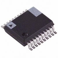
IC ENERGY METERING 1PHASE 20SSOP
Manufacturer
Analog Devices Inc
Datasheet
1.ADE7753ARSZ.pdf
(60 pages)
Specifications of ADE7753ARSZ
Input Impedance
390 KOhm
Measurement Error
0.1%
Voltage - I/o High
2.4V
Voltage - I/o Low
0.8V
Current - Supply
3mA
Voltage - Supply
4.75 V ~ 5.25 V
Operating Temperature
-40°C ~ 85°C
Mounting Type
Surface Mount
Package / Case
20-SSOP (0.200", 5.30mm Width)
Meter Type
Single Phase
Ic Function
Single-Phase Multifunction Metering IC
Supply Voltage Range
4.75V To 5.25V
Operating Temperature Range
-40°C To +85°C
Digital Ic Case Style
SSOP
No. Of Pins
20
Lead Free Status / RoHS Status
Lead free / RoHS Compliant
For Use With
EVAL-ADE7753ZEB - BOARD EVALUATION AD7753
Lead Free Status / RoHS Status
Lead free / RoHS Compliant, Lead free / RoHS Compliant
Available stocks
Company
Part Number
Manufacturer
Quantity
Price

Part Number:
ADE7753ARSZ
Manufacturer:
ADI/亚德诺
Quantity:
20 000
Part Number:
ADE7753ARSZRL
Manufacturer:
ADI/亚德诺
Quantity:
20 000


ADE7753
Parameter
ON-CHIP REFERENCE
CLKIN
LOGIC INPUTS
LOGIC OUTPUTS
POWER SUPPLY
_______________________________________________
1
2
3
See the plots in the Typical Performance Characteristics section.
See the Terminology section for explanation of specifications.
See the Analog Inputs section.
RESET , DIN, SCLK, CLKIN, and CS
Input High Voltage, V
Input Low Voltage, V
Input Current, I
Input Capacitance, C
Channel 2
REFERENCE INPUT
REF
Input Capacitance
Reference Error
Current Source
Output Impedance
Temperature Coefficient
Input Clock Frequency
SAG and IRQ
Output High Voltage, V
Output Low Voltage, V
ZX and DOUT
Output High Voltage, V
Output Low Voltage, V
CF
Output High Voltage, V
Output Low Voltage, V
AVDD
DVDD
AI
DI
DD
DD
IN/OUT
Signal-to-Noise Plus Distortion
Bandwidth (–3 dB)
Input Voltage Range
IN
INL
IN
INH
OL
OL
OL
OH
OH
OH
Spec
60
140
2.6
2.2
10
±200
10
3.4
30
4
1
2.4
0.8
±3
10
4
0.4
4
0.4
4
1
4.75
5.25
4.75
5.25
3
4
OUTPUT
Figure 2. Load Circuit for Timing Specifications
PIN
TO
Unit
dB typ
Hz
V max
V min
pF max
mV max
µA max
kΩ min
ppm/°C typ
MHz max
MHz min
V min
V max
µA max
pF max
V min
V max
V min
V max
V min
V max
V min
V max
V min
V max
mA max
mA max
50pF
Rev. A | Page 4 of 60
C
L
200 µA
1.6mA
For specified performance
Test Conditions/Comments
See the Channel 2 Sampling section
150 mV rms/60 Hz, gain = 2
CLKIN = 3.579545 MHz
2.4 V + 8%
2.4 V – 8%
Nominal 2.4 V at REF
All specifications CLKIN of 3.579545 MHz
DV
DV
Typically 10 nA, V
Open-drain outputs, 10 kΩ pull-up resistor
I
I
I
I
I
I
5 V – 5%
5 V + 5%
5 V – 5%
5 V + 5%
Typically 2.0 mA
Typically 3.0 mA
SOURCE
SINK
SOURCE
SINK
SOURCE
SINK
I
I
Ol
OH
DD
DD
= 0.8 mA
= 7 mA
= 0.8 mA
= 5 V ± 10%
= 5 V ± 10%
= 5 mA
= 5 mA
= 5 mA
02875-0-002
+2.1V
IN
= 0 V to DV
IN/OUT
pin
DD
Related parts for ADE7753ARSZ
Image
Part Number
Description
Manufacturer
Datasheet
Request
R

Part Number:
Description:
±1.7g Dual-Axis IMEMS Accelerometer Evaluation Board
Manufacturer:
Analog Devices Inc
Datasheet:

Part Number:
Description:
Inertial Sensor Evaluation System
Manufacturer:
Analog Devices Inc
Datasheet:
Part Number:
Description:
Manufacturer:
Analog Devices Inc
Datasheet:
Part Number:
Description:
Manufacturer:
Analog Devices Inc
Datasheet:
Part Number:
Description:
Manufacturer:
Analog Devices Inc
Datasheet:
Part Number:
Description:
Manufacturer:
Analog Devices Inc
Datasheet:
Part Number:
Description:
Manufacturer:
Analog Devices Inc
Datasheet:
Part Number:
Description:
Manufacturer:
Analog Devices Inc
Datasheet:
Part Number:
Description:
Manufacturer:
Analog Devices Inc
Datasheet:
Part Number:
Description:
Manufacturer:
Analog Devices Inc
Datasheet:
Part Number:
Description:
Manufacturer:
Analog Devices Inc
Datasheet:
Part Number:
Description:
Manufacturer:
Analog Devices Inc
Datasheet:
Part Number:
Description:
Manufacturer:
Analog Devices Inc
Datasheet: