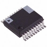
ADE7763ARS Analog Devices Inc, ADE7763ARS Datasheet - Page 23

ADE7763ARS
Manufacturer Part Number
ADE7763ARS
Description
IC ENERGY METER 1PHASE 20SSOP
Manufacturer
Analog Devices Inc
Specifications of ADE7763ARS
Input Impedance
390 KOhm
Measurement Error
0.1%
Voltage - I/o High
2.4V
Voltage - I/o Low
0.8V
Current - Supply
3mA
Voltage - Supply
4.75 V ~ 5.25 V
Operating Temperature
-40°C ~ 85°C
Mounting Type
Surface Mount
Package / Case
20-SSOP (0.200", 5.30mm Width)
Meter Type
Single Phase
For Use With
EVAL-ADE7763ZEB - BOARD EVALUATION FOR ADE7763
Lead Free Status / RoHS Status
Contains lead / RoHS non-compliant
Available stocks
Company
Part Number
Manufacturer
Quantity
Price
Part Number:
ADE7763ARS
Manufacturer:
ADI/亚德诺
Quantity:
20 000
Part Number:
ADE7763ARSZ
Manufacturer:
ADI/亚德诺
Quantity:
20 000
Part Number:
ADE7763ARSZRL
Manufacturer:
ADI/亚德诺
Quantity:
20 000
Channel 2 has only one analog input range (0.5 V differential).
Like Channel 1, Channel 2 has a PGA with gain selections of 1,
2, 4, 8, and 16. For energy measurement, the output of the ADC
is passed directly to the multiplier and is not filtered. An HPF is
not required to remove any dc offset; it is only required that the
offset is removed from one channel to eliminate errors caused
by offsets in the power calculation. In waveform sampling mode,
one of four output sample rates can be chosen by using Bits 11
and 12 of the mode register. The available output sample rates
are 27.9 kSPS, 14 kSPS, 7 kSPS, or 3.5 kSPS—see the Mode
Register (0X09) section. The interrupt request output IRQ
indicates that a sample is available by going active low. The
timing is the same as that for Channel 1, as shown in Figure 44.
Channel 2 RMS Calculation
Figure 48 shows the details of the signal processing chain for the
rms calculation on Channel 2. The Channel 2 rms value is
processed from the samples used in the Channel 2 waveform
sampling mode. The rms value is slightly attenuated due to
LPF1. The Channel 2 rms value is stored in the unsigned, 24-bit
VRMS register. The update rate of the Channel 2 rms
measurement is CLKIN/4.
With the specified full-scale ac analog input signal of 0.5 V, the
output from LPF1 swings between 0x2518 and 0xDAE8 at
60 Hz—see the Channel 2 ADC section. The equivalent rms
value of this full-scale ac signal is approximately 1,561,400
(0x17 D338) in the VRMS register. The voltage rms measure-
ment provided in the ADE7763 is accurate to within ±0.5% for
signal input between full scale and full scale/20. The conversion
from the register value to volts must be done externally in the
CHANNEL 2
ANALOG
INPUT RANGE
0.5V, 0.25V, 0.125V,
62.5mV, 31.25mV
V2
V2N
V2P
LPF1
0V
V1
0xDAE8
VOLTAGE SIGNAL (V(t))
×1, ×2, ×4,
×8, ×16
0x2518
Figure 47. ADC and Signal Processing in Channel 2
PGA2
0x0
Figure 48. Channel 2 RMS Signal Processing
{GAIN[7:5]}
REFERENCE
Rev. A | Page 23 of 56
ADC 2
2.42V
0xDAE8
0xD7AE
0x2852
0x2581
0x0000
LPF3
WORD RANGE
LPF OUTPUT
microprocessor using a volts/LSB constant. Because the low-pass
filter used for calculating the rms value is imperfect, there is some
ripple noise from 2ω term present in the rms measurement. To
minimize the effect of noise in the reading, synchronize the rms
reading with the zero crossings of the voltage input.
Channel 2 RMS Offset Compensation
The ADE7763 incorporates a Channel 2 rms offset
compensation register (VRMSOS). This is a 12-bit, signed
register that can be used to remove offset in the Channel 2 rms
calculation. An offset could exist in the rms calculation due to
input noises and dc offset in the input samples. The offset
calibration allows the contents of the VRMS register to be
maintained at 0 when no voltage is applied. One LSB of the
Channel 2 rms offset is equivalent to 1 LSB of the rms register.
Assuming that the maximum value of the Channel 2 rms
calculation is 1,561,400d with full-scale ac inputs, then 1 LSB of
the Channel 2 rms offset represents 0.064% of measurement
error at –60 dB down of full scale.
where VRMS
correction.
The voltage rms offset compensation should be done by testing
the rms results at two nonzero input levels. One measurement
can be done close to full scale and the other at approximately
full scale/10. The voltage offset compensation can be derived
from these measurements. If the voltage rms offset register does
not have enough range, the CH2OS register can also be used.
LPF1
sgn
VRMS = VRMS
VRMOS[11:0]
2
9
2
8
+
2
0
2
+
is the rms measurement without offset
2
ACTIVE AND REACTIVE
ENERGY CALCULATION
VRMS CALCULATION
AND WAVEFORM
SAMPLING
(PEAK/SAG/ZX)
1
0x17D338
2
0
0
0x00
VRMS[23:0]
+ VRMSOS
ADE7763
(6)


